

LCMXO2-2000HE-6MG132C
Product Overview
Category
The LCMXO2-2000HE-6MG132C belongs to the category of Field-Programmable Gate Arrays (FPGAs).
Use
This FPGA is commonly used in various electronic applications that require programmable logic devices. It provides designers with flexibility and versatility in implementing digital circuits.
Characteristics
- High-density FPGA with 2000 Look-Up Tables (LUTs)
- Low power consumption
- Small form factor
- High-speed performance
- Easy to program and reconfigure
Package
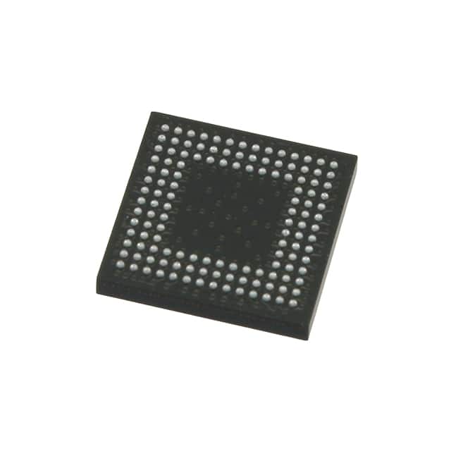
The LCMXO2-2000HE-6MG132C comes in a compact package, which ensures easy integration into electronic systems. The package type is MG132C.
Essence
The essence of this FPGA lies in its ability to be programmed and reprogrammed to perform different functions, making it suitable for a wide range of applications.
Packaging/Quantity
The LCMXO2-2000HE-6MG132C is typically packaged individually and is available in various quantities depending on the manufacturer's specifications.
Specifications
- Number of Logic Cells: 2000
- Number of Inputs/Outputs: 132
- Maximum Frequency: 100 MHz
- Operating Voltage: 1.2V
- Operating Temperature Range: -40°C to 85°C
- Configuration Memory: Flash-based
Detailed Pin Configuration
The LCMXO2-2000HE-6MG132C has a total of 132 pins, each serving a specific purpose in the FPGA's functionality. The pin configuration includes input/output pins, power supply pins, clock pins, and configuration pins. A detailed pinout diagram can be found in the product datasheet.
Functional Features
- Programmable logic cells for implementing custom digital circuits
- Dedicated input/output pins for interfacing with external devices
- Clock management resources for synchronous circuit design
- On-chip memory blocks for data storage and retrieval
- Built-in configuration memory for easy reprogramming
Advantages and Disadvantages
Advantages
- Flexibility in designing and implementing custom logic functions
- High-density integration of logic cells
- Low power consumption compared to traditional ASICs
- Easy reconfiguration for iterative design processes
- Cost-effective solution for prototyping and low-volume production
Disadvantages
- Limited performance compared to dedicated ASICs for specific applications
- Higher cost per unit compared to mass-produced ASICs
- Limited support for high-speed interfaces and protocols
Working Principles
The LCMXO2-2000HE-6MG132C operates based on the principles of field-programmable gate arrays. It consists of a matrix of programmable logic cells interconnected through configurable routing resources. The functionality of the FPGA is determined by the configuration data stored in its memory. During operation, the FPGA executes the programmed logic functions based on the input signals received.
Detailed Application Field Plans
The LCMXO2-2000HE-6MG132C finds applications in various fields, including:
- Embedded Systems: Used for implementing control and communication functions in embedded systems.
- Digital Signal Processing: Employed for real-time signal processing tasks such as filtering, modulation, and demodulation.
- Communications: Utilized in networking equipment for protocol handling and data packet processing.
- Industrial Automation: Integrated into industrial control systems for process monitoring and control.
- Consumer Electronics: Incorporated into consumer devices for user interface control and multimedia processing.
Detailed and Complete Alternative Models
There are several alternative models available in the market that offer similar functionality to the LCMXO2-2000HE-6MG132C. Some notable alternatives include:
- Xilinx Spartan-6 FPGA
- Altera Cyclone IV FPGA
- Microsemi IGLOO2 FPGA
- Intel MAX 10 FPGA
These alternative models provide varying levels of performance, capacity, and features, allowing designers to choose the most suitable option for their specific application requirements.
In conclusion, the LCMXO2-2000HE-6MG132C is a high-density FPGA that offers flexibility, low power consumption, and easy programmability. It finds applications in various fields, including embedded systems, digital signal processing, communications, industrial automation, and consumer electronics. While it has advantages such as versatility and cost-effectiveness, it also has limitations in terms of performance and cost compared to dedicated ASICs. Designers can consider alternative models based on their specific needs and requirements.
قم بإدراج 10 أسئلة وإجابات شائعة تتعلق بتطبيق LCMXO2-2000HE-6MG132C في الحلول التقنية
Sure! Here are 10 common questions and answers related to the application of LCMXO2-2000HE-6MG132C in technical solutions:
Q: What is the LCMXO2-2000HE-6MG132C? A: The LCMXO2-2000HE-6MG132C is a low-cost, low-power FPGA (Field-Programmable Gate Array) device manufactured by Lattice Semiconductor.
Q: What are the key features of the LCMXO2-2000HE-6MG132C? A: Some key features include 2000 Look-Up Tables (LUTs), 64 Kbits of embedded block RAM, 34 user I/O pins, and support for various I/O standards.
Q: What are some typical applications of the LCMXO2-2000HE-6MG132C? A: This FPGA is commonly used in applications such as industrial control systems, consumer electronics, medical devices, and communication equipment.
Q: How can I program the LCMXO2-2000HE-6MG132C? A: You can program the FPGA using Lattice Diamond or Lattice Radiant software tools provided by Lattice Semiconductor.
Q: What programming languages are supported by the LCMXO2-2000HE-6MG132C? A: The FPGA can be programmed using VHDL or Verilog hardware description languages.
Q: Can I reprogram the LCMXO2-2000HE-6MG132C multiple times? A: Yes, this FPGA supports in-system programmability, allowing you to reprogram it multiple times during development or in the field.
Q: What is the power consumption of the LCMXO2-2000HE-6MG132C? A: The power consumption depends on the design and usage, but typically it operates at low power levels, making it suitable for battery-powered applications.
Q: Can I interface the LCMXO2-2000HE-6MG132C with other components or devices? A: Yes, the FPGA has multiple I/O pins that can be used to interface with other components such as sensors, displays, memory, or communication modules.
Q: Are there any development boards available for the LCMXO2-2000HE-6MG132C? A: Yes, Lattice Semiconductor provides development boards like the LCMXO2-1200HC-4TG100C, which can be used for prototyping and evaluation purposes.
Q: Where can I find more information about the LCMXO2-2000HE-6MG132C? A: You can find detailed information, datasheets, application notes, and reference designs on the official website of Lattice Semiconductor or by contacting their technical support team.
Please note that the specific details and answers may vary depending on the context and requirements of your technical solution.