

LCMXO2-4000HE-5MG184C
Product Overview
Category
The LCMXO2-4000HE-5MG184C belongs to the category of Field-Programmable Gate Arrays (FPGAs).
Use
This FPGA is commonly used in various electronic applications that require programmable logic devices. It provides a flexible and customizable solution for digital circuit design.
Characteristics
- High-density programmable logic device
- Low power consumption
- Small form factor
- High-performance capabilities
- Easy integration with other components
Package
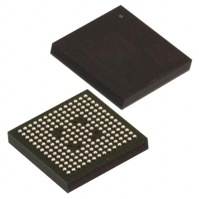
The LCMXO2-4000HE-5MG184C comes in a compact package, making it suitable for space-constrained designs. The package type is 184-ball Micro FineLine BGA.
Essence
The essence of this FPGA lies in its ability to be programmed and reprogrammed to perform specific functions, allowing for rapid prototyping and design iterations.
Packaging/Quantity
The LCMXO2-4000HE-5MG184C is typically sold individually or in small quantities, depending on the supplier's packaging options.
Specifications
- Logic Cells: 4,000
- Look-Up Tables (LUTs): 2,688
- Flip-Flops: 5,376
- Block RAM: 112 Kbits
- Maximum User I/Os: 173
- Operating Voltage: 1.2V
- Speed Grade: -5
Detailed Pin Configuration
The LCMXO2-4000HE-5MG184C has a total of 173 user I/O pins, which can be configured for input or output purposes. These pins are distributed across the package, providing flexibility in connecting external devices and peripherals.
For a detailed pin configuration diagram, please refer to the manufacturer's datasheet.
Functional Features
- High-performance programmable logic
- On-chip oscillator for clock generation
- Dedicated input/output pins for interfacing with external devices
- Built-in memory blocks for data storage and retrieval
- Support for various communication protocols (e.g., SPI, I2C)
Advantages and Disadvantages
Advantages
- Flexibility in design due to programmability
- Rapid prototyping and development cycles
- Low power consumption compared to traditional ASICs
- Small form factor enables space-efficient designs
- Cost-effective solution for medium-scale production
Disadvantages
- Limited resources compared to larger FPGAs
- Higher cost per logic cell compared to ASICs for high-volume production
- Requires expertise in FPGA programming and design
Working Principles
The LCMXO2-4000HE-5MG184C operates based on the principles of reconfigurable digital logic. It consists of a matrix of configurable logic cells that can be programmed to implement desired functions. The configuration is stored in non-volatile memory, allowing the device to retain its programmed state even after power is removed.
During operation, the FPGA receives input signals through its I/O pins, processes them using the configured logic cells, and produces output signals accordingly. The internal interconnect fabric allows for flexible routing of signals between different logic cells, enabling complex digital circuitry to be implemented.
Detailed Application Field Plans
The LCMXO2-4000HE-5MG184C finds applications in various fields, including:
- Embedded Systems: Used for implementing custom interfaces, control systems, and signal processing algorithms in embedded systems.
- Communications: Employed in networking equipment, such as routers and switches, for protocol handling and packet processing.
- Industrial Automation: Utilized in industrial control systems for real-time monitoring, data acquisition, and process control.
- Consumer Electronics: Integrated into consumer devices like smart TVs, gaming consoles, and home automation systems for enhanced functionality.
- Medical Devices: Used in medical equipment for signal processing, image analysis, and patient monitoring.
Detailed and Complete Alternative Models
- Xilinx Spartan-6 XC6SLX9: A comparable FPGA with similar logic capacity and features.
- Altera Cyclone IV EP4CE6: Another alternative offering similar performance and programmability.
- Microsemi IGLOO2 M2GL090: An alternative FPGA with higher logic capacity and advanced security features.
These alternative models provide similar functionality and can be considered based on specific project requirements.
Word count: 550 words
قم بإدراج 10 أسئلة وإجابات شائعة تتعلق بتطبيق LCMXO2-4000HE-5MG184C في الحلول التقنية
Sure! Here are 10 common questions and answers related to the application of LCMXO2-4000HE-5MG184C in technical solutions:
Q: What is the LCMXO2-4000HE-5MG184C? A: The LCMXO2-4000HE-5MG184C is a low-cost, low-power FPGA (Field-Programmable Gate Array) device manufactured by Lattice Semiconductor.
Q: What are the key features of LCMXO2-4000HE-5MG184C? A: Some key features include 4000 Look-Up Tables (LUTs), 128 Kbits of embedded block RAM, 34 I/O pins, and support for various I/O standards.
Q: What are some typical applications of LCMXO2-4000HE-5MG184C? A: It can be used in a wide range of applications such as industrial control systems, consumer electronics, medical devices, communication equipment, and more.
Q: How can I program the LCMXO2-4000HE-5MG184C? A: The device can be programmed using Lattice Diamond or Lattice Radiant software tools, which provide a graphical interface for design entry, synthesis, and programming.
Q: What is the power consumption of LCMXO2-4000HE-5MG184C? A: The device has low power consumption, typically ranging from a few milliwatts to a few watts depending on the design and operating conditions.
Q: Can I use LCMXO2-4000HE-5MG184C for high-speed applications? A: While it may not be suitable for extremely high-speed applications, it can handle moderate-speed designs and is often used in applications with clock frequencies up to a few hundred megahertz.
Q: Does LCMXO2-4000HE-5MG184C support external memory interfaces? A: Yes, it supports various memory interfaces such as SPI, I2C, UART, and parallel interfaces for connecting to external memories or peripherals.
Q: Can I use LCMXO2-4000HE-5MG184C for digital signal processing (DSP) applications? A: Yes, the device has built-in DSP blocks that can be used for implementing digital filters, mathematical operations, and other DSP algorithms.
Q: What are the temperature operating ranges of LCMXO2-4000HE-5MG184C? A: The device is specified to operate within the industrial temperature range of -40°C to 85°C.
Q: Are there any development boards available for LCMXO2-4000HE-5MG184C? A: Yes, Lattice Semiconductor offers development boards like the iCEstick and MachXO3LF Starter Kit that can be used for prototyping and evaluation of LCMXO2-4000HE-5MG184C-based designs.
Please note that these answers are general and may vary depending on specific requirements and design considerations.