

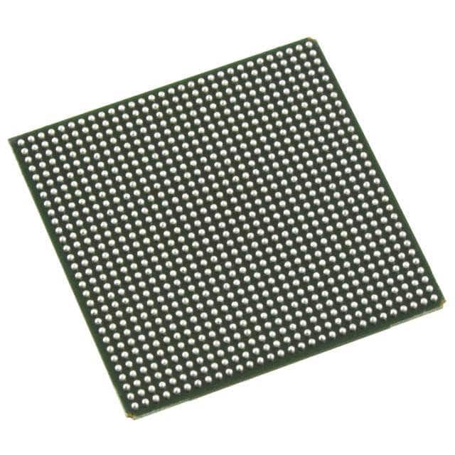
LFE2M100SE-7FN900C
Product Overview
Category
The LFE2M100SE-7FN900C belongs to the category of Field Programmable Gate Arrays (FPGAs).
Use
This FPGA is primarily used for digital logic design and implementation in various electronic systems.
Characteristics
- High-performance programmable logic device
- Offers flexibility and reconfigurability
- Provides a wide range of logic gates, flip-flops, and memory blocks
- Supports complex digital circuit designs
Package
The LFE2M100SE-7FN900C comes in a compact and durable package suitable for integration into electronic systems.
Essence
The essence of this FPGA lies in its ability to provide a customizable hardware platform that allows designers to implement complex digital circuits efficiently.
Packaging/Quantity
The LFE2M100SE-7FN900C is typically packaged individually and is available in various quantities depending on the manufacturer's specifications.
Specifications
- Model: LFE2M100SE-7FN900C
- Logic Elements: 100,000
- Speed Grade: 7
- Number of I/O Pins: 900
- Operating Voltage: 1.2V
- Maximum Frequency: 400 MHz
- Configuration Memory: Flash-based
Detailed Pin Configuration
The LFE2M100SE-7FN900C has 900 I/O pins, each serving a specific purpose in the digital circuit design. The pin configuration can be found in the product datasheet provided by the manufacturer.
Functional Features
- High-speed data processing capabilities
- Support for various communication protocols
- On-chip memory resources for efficient data storage
- Configurable I/O standards for compatibility with different interfaces
- Built-in clock management resources for precise timing control
Advantages and Disadvantages
Advantages
- Flexibility and reconfigurability enable rapid prototyping and design iterations
- High-performance capabilities suitable for demanding applications
- Wide range of I/O pins allows for versatile connectivity options
- Flash-based configuration memory ensures reliable and secure programming
Disadvantages
- Steep learning curve for beginners due to the complexity of FPGA design
- Higher power consumption compared to fixed-function integrated circuits
- Costlier than traditional microcontrollers for small-scale projects
Working Principles
The LFE2M100SE-7FN900C operates based on the principles of digital logic design. It consists of configurable logic blocks, interconnect resources, and I/O elements. The user designs a digital circuit using a hardware description language (HDL) and programs it onto the FPGA. The FPGA then configures its internal resources to implement the desired circuit functionality.
Detailed Application Field Plans
The LFE2M100SE-7FN900C finds applications in various fields, including:
- Telecommunications: Used in base stations, routers, and network switches for high-speed data processing.
- Aerospace and Defense: Employed in radar systems, avionics, and military communication equipment for their performance and reliability.
- Industrial Automation: Utilized in control systems, robotics, and machine vision applications for real-time data processing and control.
- Medical Devices: Integrated into medical imaging systems, patient monitoring devices, and laboratory equipment for advanced signal processing and data analysis.
Detailed and Complete Alternative Models
- Xilinx Virtex UltraScale+ VU9P: Offers higher logic capacity and faster performance.
- Intel Stratix 10 GX: Provides advanced features like transceiver technology and high-speed interfaces.
- Microsemi PolarFire FPGA: Known for low power consumption and security features.
These alternative models offer similar functionalities to the LFE2M100SE-7FN900C and can be considered based on specific project requirements.
Word count: 514 words
قم بإدراج 10 أسئلة وإجابات شائعة تتعلق بتطبيق LFE2M100SE-7FN900C في الحلول التقنية
Sure! Here are 10 common questions and answers related to the application of LFE2M100SE-7FN900C in technical solutions:
Q: What is the LFE2M100SE-7FN900C? A: The LFE2M100SE-7FN900C is a specific model of Field Programmable Gate Array (FPGA) manufactured by Lattice Semiconductor.
Q: What are the key features of the LFE2M100SE-7FN900C? A: Some key features of this FPGA include 100,000 logic elements, low power consumption, high-speed performance, and support for various I/O standards.
Q: In what applications can the LFE2M100SE-7FN900C be used? A: This FPGA can be used in a wide range of applications such as industrial automation, telecommunications, automotive systems, medical devices, and more.
Q: How does the LFE2M100SE-7FN900C differ from other FPGAs? A: The LFE2M100SE-7FN900C stands out due to its low power consumption, high logic element count, and support for various I/O standards, making it suitable for demanding applications.
Q: What development tools are available for programming the LFE2M100SE-7FN900C? A: Lattice Semiconductor provides the Lattice Diamond design software suite, which includes tools for designing, simulating, and programming the FPGA.
Q: Can the LFE2M100SE-7FN900C be reprogrammed after deployment? A: Yes, the LFE2M100SE-7FN900C is a field-programmable device, meaning it can be reprogrammed even after it has been deployed in a system.
Q: What are the power requirements for the LFE2M100SE-7FN900C? A: The power requirements vary depending on the specific application and configuration, but typically it operates at low voltages (e.g., 1.2V) and consumes relatively low power.
Q: Can the LFE2M100SE-7FN900C interface with other components or devices? A: Yes, the FPGA supports various I/O standards, allowing it to interface with different components and devices such as sensors, memory modules, communication interfaces, etc.
Q: Are there any limitations or considerations when using the LFE2M100SE-7FN900C? A: Some considerations include the need for proper cooling due to high-speed operation, understanding the FPGA's architecture and programming flow, and ensuring compatibility with other system components.
Q: Where can I find more information about the LFE2M100SE-7FN900C? A: You can find more detailed information, datasheets, reference designs, and application notes on the official website of Lattice Semiconductor or by contacting their technical support team.