

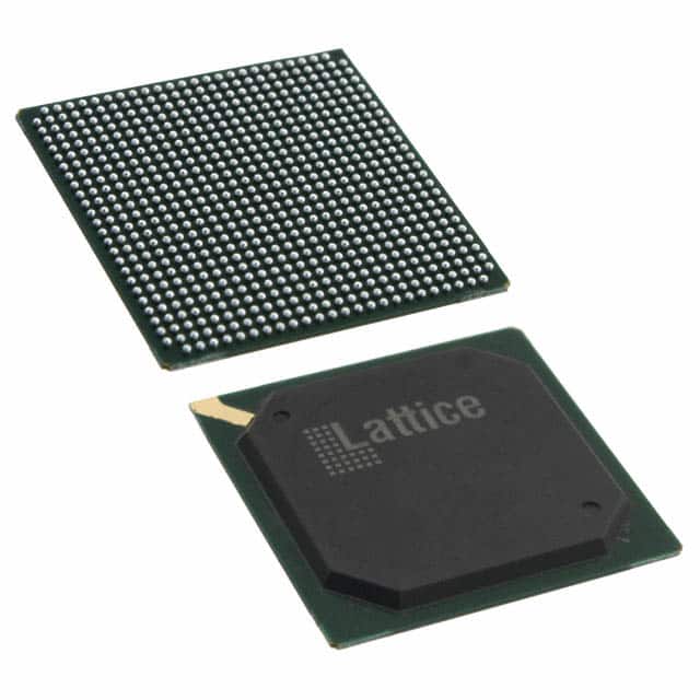
LFE2M35SE-5FN672I
Product Overview
Category
The LFE2M35SE-5FN672I belongs to the category of Field Programmable Gate Arrays (FPGAs).
Use
FPGAs are integrated circuits that can be programmed and reprogrammed to perform various digital functions. The LFE2M35SE-5FN672I is specifically designed for applications requiring high-performance and low-power consumption.
Characteristics
- High performance: The LFE2M35SE-5FN672I offers fast processing speeds and efficient data handling capabilities.
- Low power consumption: This FPGA is designed to minimize power usage, making it suitable for battery-powered devices.
- Versatility: It can be programmed to perform a wide range of digital functions, making it adaptable to different applications.
Package and Quantity
The LFE2M35SE-5FN672I comes in a specific package type known as a 672-ball FineLine BGA (Ball Grid Array). Each package contains one unit of the FPGA.
Specifications
- Device family: LatticeECP2M
- Logic elements: 35,000
- Speed grade: -5
- Number of I/O pins: 672
- Operating voltage: 1.2V
- Package dimensions: 23mm x 23mm
Pin Configuration
The detailed pin configuration of the LFE2M35SE-5FN672I can be found in the product datasheet provided by the manufacturer.
Functional Features
- High-speed data processing: The FPGA's architecture allows for efficient handling of large amounts of data at high speeds.
- Flexible programming: The LFE2M35SE-5FN672I can be programmed using various hardware description languages (HDLs) such as VHDL or Verilog.
- On-chip memory: It includes embedded memory blocks that can be used for data storage and retrieval.
- Configurable I/Os: The FPGA offers a wide range of configurable input/output pins, allowing for easy interfacing with external devices.
Advantages
- Customizability: FPGAs provide the flexibility to implement custom logic functions tailored to specific application requirements.
- Time-to-market: Using an FPGA can significantly reduce development time compared to designing custom ASICs (Application-Specific Integrated Circuits).
- Cost-effectiveness: FPGAs offer a cost-effective solution for prototyping and low-volume production runs.
Disadvantages
- Complexity: Designing and programming FPGAs requires specialized knowledge and expertise.
- Power consumption: While efforts have been made to minimize power usage, FPGAs generally consume more power compared to dedicated hardware solutions.
- Limited performance optimization: FPGAs may not achieve the same level of performance as dedicated ASICs for certain applications.
Working Principles
FPGAs consist of an array of programmable logic elements interconnected by configurable routing resources. These logic elements can be programmed to perform various digital functions, such as arithmetic operations, data processing, and control tasks. The configuration of the FPGA determines the behavior and functionality of the circuit.
Application Field Plans
The LFE2M35SE-5FN672I is suitable for a wide range of applications, including: - Communications systems - Industrial automation - Medical devices - Automotive electronics - Aerospace and defense
Alternative Models
There are several alternative models available in the market that offer similar functionality to the LFE2M35SE-5FN672I. Some notable alternatives include: - Xilinx Virtex-7 series - Intel (formerly Altera) Cyclone V series - Microsemi SmartFusion2 series
These alternative models should be evaluated based on specific application requirements and design constraints.
In conclusion, the LFE2M35SE-5FN672I is a high-performance FPGA with low power consumption, offering versatility and flexibility for various digital applications. Its customizable nature and cost-effectiveness make it an attractive choice for designers seeking programmable logic solutions.
Word count: 511
قم بإدراج 10 أسئلة وإجابات شائعة تتعلق بتطبيق LFE2M35SE-5FN672I في الحلول التقنية
Sure! Here are 10 common questions and answers related to the application of LFE2M35SE-5FN672I in technical solutions:
Question: What is the LFE2M35SE-5FN672I?
Answer: The LFE2M35SE-5FN672I is a specific model of Field-Programmable Gate Array (FPGA) manufactured by Lattice Semiconductor.Question: What are the key features of the LFE2M35SE-5FN672I?
Answer: Some key features of this FPGA include 35,000 Look-Up Tables (LUTs), 672-pin FineLine BGA package, 5V tolerant I/Os, and low power consumption.Question: What are the typical applications of the LFE2M35SE-5FN672I?
Answer: This FPGA is commonly used in various technical solutions such as industrial automation, telecommunications, automotive electronics, medical devices, and more.Question: How can I program the LFE2M35SE-5FN672I?
Answer: You can program this FPGA using the Lattice Diamond design software or other compatible programming tools provided by Lattice Semiconductor.Question: What is the maximum operating frequency of the LFE2M35SE-5FN672I?
Answer: The maximum operating frequency of this FPGA depends on the specific design and implementation, but it can typically reach frequencies of several hundred megahertz.Question: Can I interface the LFE2M35SE-5FN672I with other components or peripherals?
Answer: Yes, this FPGA supports various standard interfaces such as SPI, I2C, UART, GPIO, and more, allowing you to easily interface with other components or peripherals.Question: Does the LFE2M35SE-5FN672I support high-speed serial communication protocols?
Answer: Yes, this FPGA supports high-speed serial protocols like PCIe, SATA, USB, and Ethernet, making it suitable for applications requiring fast data transfer.Question: What is the power supply requirement for the LFE2M35SE-5FN672I?
Answer: This FPGA operates at a nominal core voltage of 1.2V and requires additional power supplies for I/O banks, which can range from 1.2V to 3.3V depending on the specific requirements.Question: Can I use the LFE2M35SE-5FN672I in harsh environments?
Answer: Yes, this FPGA is designed to operate reliably in industrial-grade temperature ranges and can withstand harsh environmental conditions.Question: Where can I find more information about the LFE2M35SE-5FN672I?
Answer: You can find detailed technical documentation, datasheets, application notes, and reference designs on the official website of Lattice Semiconductor or by contacting their customer support.