

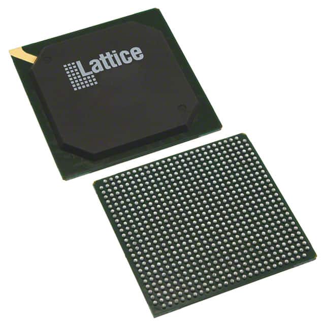
LFE3-95EA-8LFN672I
Product Overview
Category
The LFE3-95EA-8LFN672I belongs to the category of Field Programmable Gate Arrays (FPGAs).
Use
FPGAs are integrated circuits that can be programmed and reprogrammed to perform various digital functions. The LFE3-95EA-8LFN672I is specifically designed for high-performance applications that require complex logic functions.
Characteristics
- High-performance FPGA with advanced features
- Flexible and reprogrammable design
- Supports complex logic functions
- Offers high-speed data processing capabilities
Package
The LFE3-95EA-8LFN672I comes in a compact package that ensures easy integration into electronic systems. It is designed to be mounted on a printed circuit board (PCB) using surface mount technology (SMT).
Essence
The essence of the LFE3-95EA-8LFN672I lies in its ability to provide a customizable and versatile solution for implementing complex digital logic functions in high-performance applications.
Packaging/Quantity
The LFE3-95EA-8LFN672I is typically packaged in reels or trays, depending on the manufacturer's specifications. The quantity per package may vary, but it is commonly available in quantities suitable for both prototyping and production purposes.
Specifications
- FPGA Family: LatticeECP3
- Logic Elements: 95,000
- Speed Grade: -8
- Number of I/Os: 672
- Operating Voltage: 1.2V
- Package Type: FCBGA
Detailed Pin Configuration
The LFE3-95EA-8LFN672I has a total of 672 pins, which are assigned to various functions such as input/output (I/O), power supply, configuration, and clock signals. The pin configuration may vary depending on the specific application requirements and the chosen package.
Functional Features
- High-performance FPGA architecture
- Configurable logic blocks (CLBs) for implementing complex logic functions
- Dedicated memory blocks for efficient data storage
- Built-in high-speed I/O interfaces for seamless communication with external devices
- Flexible clock management resources for precise timing control
- On-chip configuration memory for easy reprogramming
Advantages and Disadvantages
Advantages
- Versatile and customizable solution for complex digital logic functions
- High-performance capabilities suitable for demanding applications
- Reprogrammable design allows for iterative development and updates
- Compact package enables easy integration into electronic systems
Disadvantages
- Steeper learning curve compared to traditional fixed-function integrated circuits
- Higher cost compared to simpler logic devices for less demanding applications
- Requires specialized design tools and expertise for efficient utilization
Working Principles
The LFE3-95EA-8LFN672I operates based on the principles of field-programmable gate arrays. It consists of configurable logic blocks (CLBs), interconnect resources, memory blocks, I/O interfaces, and other supporting components. The CLBs can be programmed to implement various logic functions, while the interconnect resources enable the routing of signals between different blocks. The memory blocks provide storage for data, and the I/O interfaces facilitate communication with external devices. By configuring these elements, the FPGA can perform complex digital operations according to the desired functionality.
Detailed Application Field Plans
The LFE3-95EA-8LFN672I finds applications in a wide range of fields that require high-performance digital processing capabilities. Some potential application areas include:
- Telecommunications: The FPGA can be used in network equipment, such as routers and switches, to handle high-speed data processing and protocol conversions.
- Aerospace and Defense: The FPGA can be employed in radar systems, communication satellites, and military equipment for signal processing, encryption, and control functions.
- Industrial Automation: The FPGA can be utilized in programmable logic controllers (PLCs) and robotic systems to implement complex control algorithms and real-time data processing.
- Medical Devices: The FPGA can be integrated into medical imaging systems, patient monitoring devices, and laboratory equipment to enable high-speed data acquisition and processing.
- Automotive Electronics: The FPGA can be employed in advanced driver assistance systems (ADAS), infotainment systems, and engine control units (ECUs) for efficient data processing and control.
Detailed and Complete Alternative Models
- Xilinx Virtex UltraScale+ VU9P: Another high-performance FPGA with similar capabilities and a large number of logic elements.
- Intel Stratix 10 GX: A powerful FPGA offering high-speed transceivers and advanced DSP capabilities.
- Microsemi PolarFire FPGA: A low-power FPGA suitable for applications requiring energy-efficient solutions.
- QuickLogic EOS S3: A small-sized FPGA designed for low-power edge computing applications.
- Actel ProASIC
قم بإدراج 10 أسئلة وإجابات شائعة تتعلق بتطبيق LFE3-95EA-8LFN672I في الحلول التقنية
Sure! Here are 10 common questions and answers related to the application of LFE3-95EA-8LFN672I in technical solutions:
Q: What is the LFE3-95EA-8LFN672I? A: The LFE3-95EA-8LFN672I is a field-programmable gate array (FPGA) manufactured by Lattice Semiconductor.
Q: What are the key features of the LFE3-95EA-8LFN672I? A: Some key features include 95,000 logic elements, 672-pin package, low power consumption, and high-speed performance.
Q: What are the typical applications of the LFE3-95EA-8LFN672I? A: The LFE3-95EA-8LFN672I is commonly used in various technical solutions such as telecommunications, industrial automation, automotive electronics, and medical devices.
Q: How can I program the LFE3-95EA-8LFN672I? A: The LFE3-95EA-8LFN672I can be programmed using hardware description languages (HDLs) like VHDL or Verilog, or through graphical programming tools provided by Lattice Semiconductor.
Q: What is the power supply requirement for the LFE3-95EA-8LFN672I? A: The LFE3-95EA-8LFN672I typically operates at a voltage range of 1.2V to 1.5V, depending on the specific configuration.
Q: Can the LFE3-95EA-8LFN672I interface with other components or devices? A: Yes, the LFE3-95EA-8LFN672I supports various communication interfaces such as SPI, I2C, UART, and Ethernet, allowing it to interface with other components or devices.
Q: What is the maximum operating frequency of the LFE3-95EA-8LFN672I? A: The maximum operating frequency of the LFE3-95EA-8LFN672I depends on the specific design and implementation, but it can typically reach frequencies in the range of hundreds of megahertz (MHz) to a few gigahertz (GHz).
Q: Can the LFE3-95EA-8LFN672I be reprogrammed after deployment? A: Yes, the LFE3-95EA-8LFN672I is a field-programmable device, which means it can be reprogrammed even after it has been deployed in a system.
Q: Are there any development tools available for designing with the LFE3-95EA-8LFN672I? A: Yes, Lattice Semiconductor provides development tools like Lattice Diamond and Lattice Radiant, which offer comprehensive design and verification capabilities for working with the LFE3-95EA-8LFN672I.
Q: Where can I find more information about the LFE3-95EA-8LFN672I? A: You can find more detailed information about the LFE3-95EA-8LFN672I, including datasheets, application notes, and reference designs, on the official website of Lattice Semiconductor or by contacting their technical support team.