

LFXP2-30E-7FT256C
Product Overview
Category
The LFXP2-30E-7FT256C belongs to the category of Field-Programmable Gate Arrays (FPGAs).
Use
This FPGA is commonly used in electronic circuits for various applications, such as digital signal processing, embedded systems, and high-performance computing.
Characteristics
- High flexibility: The LFXP2-30E-7FT256C offers a high level of programmability, allowing users to configure its internal logic according to their specific requirements.
- Low power consumption: This FPGA is designed to operate efficiently with low power consumption, making it suitable for battery-powered devices or energy-efficient applications.
- High-speed performance: With its advanced architecture and optimized circuitry, the LFXP2-30E-7FT256C can achieve high-speed data processing and computation.
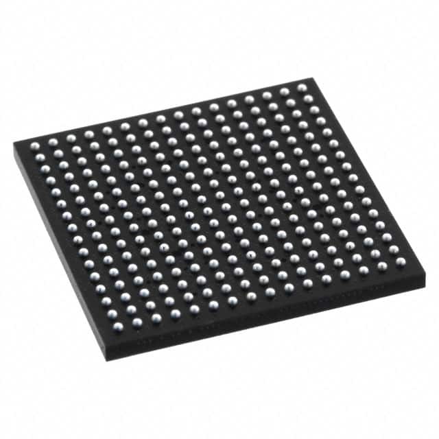
- Compact package: The FPGA comes in a 256-pin Fine-Pitch Ball Grid Array (FBGA) package, ensuring a small footprint and ease of integration into electronic designs.
- Robustness: The LFXP2-30E-7FT256C is built to withstand harsh operating conditions, including temperature variations and electrical noise.
Packaging/Quantity
The LFXP2-30E-7FT256C is typically packaged individually in an anti-static bag. It is available for purchase in both single-unit quantities and bulk orders.
Specifications
- Logic Cells: 30,000
- Look-Up Tables (LUTs): 60,000
- Flip-Flops: 120,000
- Block RAM: 1,080 Kbits
- Maximum Frequency: 400 MHz
- I/O Pins: 256
- Voltage Range: 1.2V - 3.3V
- Operating Temperature Range: -40°C to 100°C
Detailed Pin Configuration
The LFXP2-30E-7FT256C has a total of 256 I/O pins, which are configurable for various purposes. The pin configuration can be found in the manufacturer's datasheet or reference manual.
Functional Features
- Programmability: The FPGA can be programmed and reprogrammed to implement different logic functions, allowing for flexibility in system design.
- Parallel Processing: With its multiple logic cells and high-speed performance, the LFXP2-30E-7FT256C enables parallel processing of data, enhancing overall system efficiency.
- On-Chip Memory: The built-in Block RAM provides fast and efficient memory access, enabling storage and retrieval of intermediate results during computation.
- I/O Flexibility: The FPGA offers a wide range of I/O pins, supporting various communication protocols and interfacing with external devices.
Advantages and Disadvantages
Advantages
- Versatility: The LFXP2-30E-7FT256C can be used in a wide range of applications due to its programmability and flexibility.
- High Performance: This FPGA delivers high-speed processing capabilities, making it suitable for demanding computational tasks.
- Low Power Consumption: The optimized design of the LFXP2-30E-7FT256C ensures efficient power usage, reducing energy consumption in electronic systems.
Disadvantages
- Complexity: Utilizing FPGAs requires expertise in digital design and programming, which may pose a challenge for beginners or those unfamiliar with FPGA technology.
- Cost: FPGAs, including the LFXP2-30E-7FT256C, tend to be more expensive compared to other integrated circuits due to their advanced features and customization options.
Working Principles
FPGAs like the LFXP2-30E-7FT256C consist of an array of configurable logic blocks interconnected by programmable routing resources. The logic blocks can be programmed to implement desired digital functions using Hardware Description Languages (HDLs) or graphical tools. During operation, the FPGA executes the configured logic based on input signals and produces the desired output.
Detailed Application Field Plans
The LFXP2-30E-7FT256C finds applications in various fields, including:
- Communications: Used in wireless communication systems for signal processing and protocol implementation.
- Industrial Automation: Employed in control systems for real-time monitoring and process automation.
- Aerospace and Defense: Utilized in radar systems, avionics, and military-grade equipment for high-performance computing and data processing.
- Medical Devices: Integrated into medical imaging systems, patient monitoring devices, and diagnostic equipment for efficient data processing and analysis.
- Automotive: Applied in advanced driver-assistance systems (ADAS), infotainment systems, and engine control units (ECUs) for enhanced functionality and performance.
Detailed and Complete Alternative Models
- Xilinx Artix-7 XC7A35T-1CPG236C
- Intel Cyclone IV
قم بإدراج 10 أسئلة وإجابات شائعة تتعلق بتطبيق LFXP2-30E-7FT256C في الحلول التقنية
Sure! Here are 10 common questions and answers related to the application of LFXP2-30E-7FT256C in technical solutions:
Q: What is the LFXP2-30E-7FT256C? A: The LFXP2-30E-7FT256C is a field-programmable gate array (FPGA) manufactured by Lattice Semiconductor.
Q: What are the key features of the LFXP2-30E-7FT256C? A: The key features of this FPGA include 30,000 logic elements, 256-pin package, and support for various I/O standards.
Q: What applications can the LFXP2-30E-7FT256C be used for? A: This FPGA is commonly used in applications such as industrial automation, telecommunications, automotive electronics, and medical devices.
Q: How can I program the LFXP2-30E-7FT256C? A: You can program this FPGA using Lattice Diamond design software or other compatible programming tools.
Q: What voltage levels does the LFXP2-30E-7FT256C support? A: This FPGA supports various voltage levels, including 1.2V, 1.5V, 1.8V, 2.5V, and 3.3V.
Q: Can I interface the LFXP2-30E-7FT256C with external devices? A: Yes, this FPGA provides multiple I/O banks that allow you to interface with external devices using different voltage levels.
Q: Does the LFXP2-30E-7FT256C support high-speed serial communication protocols? A: Yes, this FPGA supports high-speed serial protocols such as PCIe, Gigabit Ethernet, and USB.
Q: Can I use the LFXP2-30E-7FT256C for real-time signal processing? A: Absolutely! This FPGA offers dedicated DSP blocks that can be used for efficient real-time signal processing tasks.
Q: What kind of development boards are available for the LFXP2-30E-7FT256C? A: Lattice Semiconductor provides development boards like the LatticeECP3 Versa Development Kit that support this FPGA.
Q: Where can I find technical documentation and support for the LFXP2-30E-7FT256C? A: You can find technical documentation, datasheets, application notes, and support resources on the official Lattice Semiconductor website.
Please note that the answers provided here are general and may vary depending on specific requirements and use cases.