

LFXP2-8E-5FT256C
Product Overview
Category
The LFXP2-8E-5FT256C belongs to the category of Field-Programmable Gate Arrays (FPGAs).
Use
This FPGA is commonly used in various electronic devices and systems for digital logic implementation, prototyping, and development purposes.
Characteristics
- The LFXP2-8E-5FT256C offers a high level of flexibility and reconfigurability.
- It provides a large number of programmable logic elements and configurable I/O pins.
- The FPGA supports complex digital designs and can be customized according to specific requirements.
Package
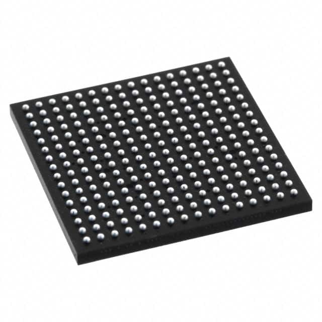
The LFXP2-8E-5FT256C comes in a compact 256-pin Fine-Pitch Ball Grid Array (FBGA) package.
Essence
The essence of the LFXP2-8E-5FT256C lies in its ability to provide a versatile platform for implementing digital circuits with high performance and flexibility.
Packaging/Quantity
The LFXP2-8E-5FT256C is typically packaged individually and is available in various quantities depending on the manufacturer's specifications.
Specifications
- Logic Cells: 8,000
- Look-Up Tables (LUTs): 16,000
- Flip-Flops: 8,000
- Block RAM: 360 Kbits
- Maximum Frequency: 400 MHz
- I/O Pins: 256
- Voltage Range: 1.2V - 3.3V
- Operating Temperature Range: -40°C to +100°C
Detailed Pin Configuration
The LFXP2-8E-5FT256C has 256 I/O pins, each of which can be configured as an input or output. These pins are organized into different banks, allowing for flexible connectivity and integration with other components.
For a detailed pin configuration diagram, please refer to the datasheet provided by the manufacturer.
Functional Features
- High-performance programmable logic elements for implementing complex digital designs.
- Configurable I/O pins for interfacing with external devices and systems.
- Dedicated clock management resources for precise timing control.
- On-chip memory blocks for efficient data storage and retrieval.
- Built-in support for various communication protocols and interfaces.
Advantages and Disadvantages
Advantages
- Flexibility: The LFXP2-8E-5FT256C offers a high level of flexibility, allowing designers to adapt and modify their digital circuits as needed.
- Reconfigurability: The FPGA can be reprogrammed multiple times, enabling rapid prototyping and iterative design processes.
- Integration: With its large number of I/O pins, the FPGA facilitates seamless integration with other electronic components and systems.
- Performance: The LFXP2-8E-5FT256C provides high-speed operation and supports complex digital designs.
Disadvantages
- Complexity: Working with FPGAs requires specialized knowledge and expertise in digital design and programming.
- Power Consumption: FPGAs tend to consume more power compared to fixed-function integrated circuits.
- Cost: FPGAs can be relatively expensive compared to other digital logic implementation options.
Working Principles
The LFXP2-8E-5FT256C operates based on the principles of configurable logic. It consists of an array of programmable logic elements interconnected through configurable routing resources. These logic elements can be programmed to implement desired digital functions using hardware description languages (HDLs) or graphical tools.
Upon programming, the FPGA's internal configuration memory is loaded, defining the functionality of each logic element and the interconnections between them. This allows the FPGA to perform specific tasks according to the programmed design.
Detailed Application Field Plans
The LFXP2-8E-5FT256C finds applications in various fields, including:
- Communications: Used in networking equipment, routers, and switches for high-speed data processing and protocol handling.
- Industrial Automation: Employed in control systems, robotics, and machine vision applications for real-time data processing and control.
- Aerospace and Defense: Utilized in radar systems, avionics, and military-grade communication systems for their high performance and reliability.
- Medical Devices: Integrated into medical imaging systems, patient monitoring devices, and laboratory equipment for signal processing and data analysis.
- Automotive: Incorporated in advanced driver-assistance systems (ADAS), infotainment systems, and engine control units for enhanced functionality and performance.
Detailed and Complete Alternative Models
- Xilinx Spartan-6 XC6SLX9 FPGA
- Altera Cyclone IV EP4CE6 FPGA
- Lattice ECP5-12K FPGA
- Microsemi SmartFusion2 M2S010 FPGA
- Intel MAX 10 10M08 FPGA
These alternative models offer similar
قم بإدراج 10 أسئلة وإجابات شائعة تتعلق بتطبيق LFXP2-8E-5FT256C في الحلول التقنية
Sure! Here are 10 common questions and answers related to the application of LFXP2-8E-5FT256C in technical solutions:
Q: What is the LFXP2-8E-5FT256C? A: The LFXP2-8E-5FT256C is a field-programmable gate array (FPGA) manufactured by Lattice Semiconductor.
Q: What are the key features of the LFXP2-8E-5FT256C? A: The key features include 8,000 Look-Up Tables (LUTs), 128 Kbits of embedded block RAM, 96 user I/O pins, and support for various communication protocols.
Q: What are some typical applications of the LFXP2-8E-5FT256C? A: The LFXP2-8E-5FT256C is commonly used in industrial automation, automotive electronics, telecommunications, medical devices, and consumer electronics.
Q: How can I program the LFXP2-8E-5FT256C? A: The LFXP2-8E-5FT256C can be programmed using Lattice Diamond or Lattice Radiant software tools, which provide a graphical interface for designing and configuring the FPGA.
Q: Can the LFXP2-8E-5FT256C be used for real-time signal processing? A: Yes, the LFXP2-8E-5FT256C is capable of performing real-time signal processing tasks due to its high-speed performance and dedicated DSP blocks.
Q: Does the LFXP2-8E-5FT256C support different communication interfaces? A: Yes, the LFXP2-8E-5FT256C supports various communication protocols such as SPI, I2C, UART, and Ethernet, making it suitable for interfacing with other devices.
Q: Can the LFXP2-8E-5FT256C be used in safety-critical applications? A: Yes, the LFXP2-8E-5FT256C is designed to meet industry standards for functional safety, making it suitable for safety-critical applications.
Q: What are the power requirements for the LFXP2-8E-5FT256C? A: The LFXP2-8E-5FT256C operates at a voltage range of 1.14V to 1.26V and requires a separate power supply for I/O pins.
Q: Can I use the LFXP2-8E-5FT256C in a low-power application? A: Yes, the LFXP2-8E-5FT256C offers power-saving features such as clock gating and dynamic power management, making it suitable for low-power applications.
Q: Are there any development boards available for the LFXP2-8E-5FT256C? A: Yes, Lattice Semiconductor provides development boards like the Lattice ECP5 Versa Board, which can be used for prototyping and evaluating designs using the LFXP2-8E-5FT256C FPGA.
Please note that the answers provided here are general and may vary depending on specific requirements and use cases.