

LTC1290CCSW#PBF
Product Overview
- Category: Integrated Circuit (IC)
- Use: Analog-to-Digital Converter (ADC)
- Characteristics: High-resolution, low-power consumption
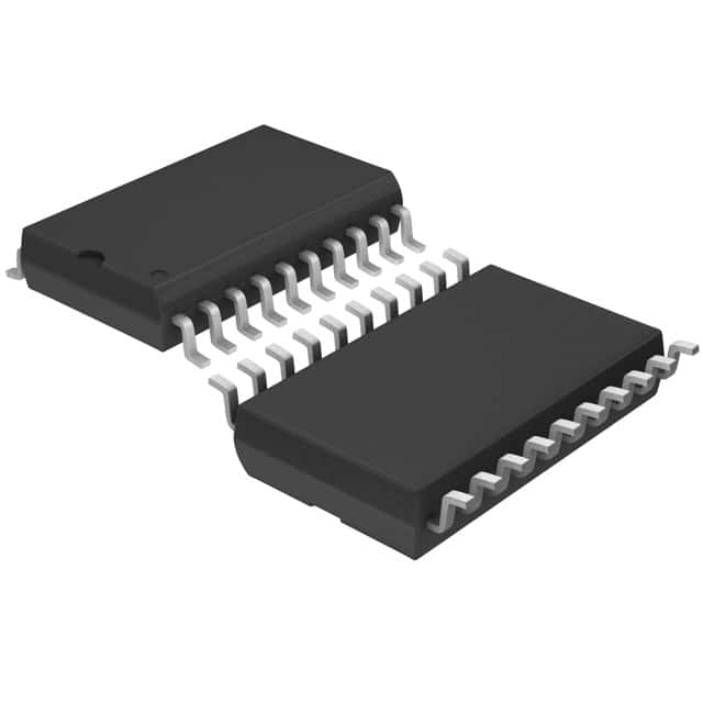
- Package: 20-pin Wide SOIC (Small Outline Integrated Circuit)
- Essence: Conversion of analog signals to digital data
- Packaging/Quantity: Tape and Reel, 250 units per reel
Specifications
- Resolution: 12 bits
- Sampling Rate: Up to 100 kSPS (Samples per Second)
- Input Voltage Range: ±10V
- Power Supply Voltage: +5V
- Power Consumption: 1.2mW (typical)
- Operating Temperature Range: -40°C to +85°C
Detailed Pin Configuration
- VREF-
- VREF+
- AGND
- VIN-
- VIN+
- REFOUT
- REFOUT/AGND
- CS
- SDO
- SDI
- SCLK
- DGND
- DOUT
- DIN
- CLK
- PD
- EOC
- INTR
- VCC
- VCC
Functional Features
- High-resolution conversion with 12-bit accuracy
- Low power consumption for energy-efficient applications
- Wide input voltage range allows for versatile signal conversion
- Serial interface for easy integration with microcontrollers
- On-chip reference voltage generator for precise measurements
- Programmable shutdown mode for power-saving operation
Advantages and Disadvantages
Advantages
- High resolution provides accurate digital representation of analog signals
- Low power consumption extends battery life in portable devices
- Versatile input voltage range accommodates various signal levels
- Serial interface simplifies communication with microcontrollers
- On-chip reference voltage generator ensures precise measurements
Disadvantages
- Limited sampling rate may not be suitable for high-speed applications
- 20-pin package may require additional board space compared to smaller packages
- Requires external components for proper operation and signal conditioning
Working Principles
The LTC1290CCSW#PBF is an analog-to-digital converter that converts continuous analog signals into discrete digital data. It utilizes a successive approximation algorithm to achieve high-resolution conversion with 12-bit accuracy. The input voltage range of ±10V allows for the conversion of a wide range of analog signals.
The device operates by comparing the input voltage to a reference voltage generated on-chip. The conversion process is controlled by a serial interface, which communicates with an external microcontroller. The converted digital data is then outputted through the serial data output pin (SDO).
Detailed Application Field Plans
The LTC1290CCSW#PBF is commonly used in various applications that require accurate analog-to-digital conversion. Some of the typical application fields include:
- Industrial Automation: Measurement and control systems, data acquisition.
- Medical Instruments: Patient monitoring, diagnostic equipment.
- Test and Measurement: Oscilloscopes, data loggers, signal analyzers.
- Communication Systems: Signal processing, base station equipment.
- Automotive Electronics: Engine control, sensor interfaces.
Detailed and Complete Alternative Models
- LTC1289CCSW#PBF: Similar specifications, 10-bit resolution.
- LTC1291CCSW#PBF: Higher resolution, 16-bit ADC.
- LTC1296CCSW#PBF: Lower power consumption, 8-bit resolution.
Note: This list is not exhaustive and other alternative models may exist from different manufacturers.
This concludes the encyclopedia entry for LTC1290CCSW#PBF.
Word Count: 510
قم بإدراج 10 أسئلة وإجابات شائعة تتعلق بتطبيق LTC1290CCSW#PBF في الحلول التقنية
Question: What is the LTC1290CCSW#PBF?
Answer: The LTC1290CCSW#PBF is a specific model of analog-to-digital converter (ADC) manufactured by Linear Technology Corporation.Question: What is the resolution of the LTC1290CCSW#PBF?
Answer: The LTC1290CCSW#PBF has a resolution of 12 bits, meaning it can represent digital values from 0 to 4095.Question: What is the operating voltage range of the LTC1290CCSW#PBF?
Answer: The LTC1290CCSW#PBF operates within a voltage range of 4.5V to 5.5V.Question: What is the maximum sampling rate of the LTC1290CCSW#PBF?
Answer: The LTC1290CCSW#PBF has a maximum sampling rate of 100 kilosamples per second (ksps).Question: Does the LTC1290CCSW#PBF support differential inputs?
Answer: Yes, the LTC1290CCSW#PBF supports both single-ended and differential inputs.Question: What is the input voltage range of the LTC1290CCSW#PBF?
Answer: The LTC1290CCSW#PBF has an input voltage range of -10V to +10V when using differential inputs.Question: Can the LTC1290CCSW#PBF operate in a low-power mode?
Answer: Yes, the LTC1290CCSW#PBF has a low-power shutdown mode that reduces power consumption when not in use.Question: Is the LTC1290CCSW#PBF suitable for battery-powered applications?
Answer: Yes, the LTC1290CCSW#PBF is designed to be used in low-power applications, making it suitable for battery-powered devices.Question: Does the LTC1290CCSW#PBF have built-in reference voltage?
Answer: No, the LTC1290CCSW#PBF requires an external reference voltage for accurate conversions.Question: What is the package type of the LTC1290CCSW#PBF?
Answer: The LTC1290CCSW#PBF is available in a 20-pin wide SOIC (Small Outline Integrated Circuit) package.