

LTC2630ACSC6-LM12#TRPBF
Product Overview
Category
The LTC2630ACSC6-LM12#TRPBF belongs to the category of digital-to-analog converters (DACs).
Use
This product is used to convert digital signals into analog voltages or currents. It finds applications in various electronic systems where precise and accurate analog outputs are required.
Characteristics
- High resolution: The LTC2630ACSC6-LM12#TRPBF offers a resolution of 12 bits, allowing for fine-grained control over the analog output.
- Low power consumption: This DAC operates at low power levels, making it suitable for battery-powered devices.
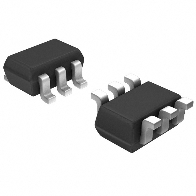
- Small package size: The LTC2630ACSC6-LM12#TRPBF comes in a small SC70-6 package, enabling its integration into space-constrained designs.
- Rail-to-rail output: It provides rail-to-rail output swing, ensuring maximum utilization of the available voltage range.
- Wide supply voltage range: This DAC can operate from a single supply voltage ranging from 2.7V to 5.5V.
Package and Quantity
The LTC2630ACSC6-LM12#TRPBF is available in an SC70-6 package. Each package contains one unit of the DAC.
Specifications
- Resolution: 12 bits
- Supply Voltage Range: 2.7V to 5.5V
- Output Type: Voltage
- Output Swing: Rail-to-Rail
- Package Type: SC70-6
Pin Configuration
The LTC2630ACSC6-LM12#TRPBF has the following pin configuration:
┌───┬───┬───┬───┬───┬───┐
   │ VDD │ VOUT │ GND │ SDA │ SCL │ CS │
   └───┴───┴───┴───┴───┴───┘
- VDD: Power supply voltage input
- VOUT: Analog output voltage
- GND: Ground reference
- SDA: Serial data input
- SCL: Serial clock input
- CS: Chip select input
Functional Features
- High accuracy: The LTC2630ACSC6-LM12#TRPBF provides excellent linearity and low integral non-linearity, ensuring accurate analog outputs.
- Fast settling time: This DAC offers a fast settling time, allowing for rapid response to changes in the digital input.
- Low glitch energy: It exhibits low glitch energy, minimizing unwanted transients during transitions.
- Internal reference: The LTC2630ACSC6-LM12#TRPBF includes an internal reference voltage, eliminating the need for an external reference source.
Advantages and Disadvantages
Advantages
- High resolution for precise analog output control
- Low power consumption for energy-efficient operation
- Small package size for easy integration into compact designs
- Wide supply voltage range for versatile applications
- Rail-to-rail output swing for maximum utilization of voltage range
Disadvantages
- Limited to voltage output only
- Single-channel configuration
Working Principles
The LTC2630ACSC6-LM12#TRPBF operates based on the principle of digital-to-analog conversion. It accepts digital input data and converts it into a corresponding analog voltage output. This conversion is achieved through a combination of internal circuitry and reference voltages. The digital input is processed, and the resulting analog voltage is available at the VOUT pin.
Detailed Application Field Plans
The LTC2630ACSC6-LM12#TRPBF can be used in various applications, including but not limited to: - Industrial automation systems - Test and measurement equipment - Audio processing devices - Programmable power supplies - Data acquisition systems
Detailed and Complete Alternative Models
- LTC2630ACSC6-LM10#TRPBF: 10-bit resolution DAC with similar features and package.
- LTC2630ACSC6-LM8#TRPBF: 8-bit resolution DAC with similar features and package.
- LTC2630ACSC6-LM14#TRPBF: 14-bit resolution DAC with similar features and package.
These alternative models provide different resolutions to suit specific application requirements while maintaining compatibility with the LTC2630ACSC6-LM12#TRPBF in terms of pin configuration and package type.
In conclusion, the LTC2630ACSC6-LM12#TRPBF is a high-resolution digital-to-analog converter with low power consumption and a small package size. It offers rail-to-rail output swing and operates over a wide supply voltage range. While it has advantages such as high accuracy and fast
قم بإدراج 10 أسئلة وإجابات شائعة تتعلق بتطبيق LTC2630ACSC6-LM12#TRPBF في الحلول التقنية
Sure! Here are 10 common questions and answers related to the application of LTC2630ACSC6-LM12#TRPBF in technical solutions:
Q: What is LTC2630ACSC6-LM12#TRPBF? A: LTC2630ACSC6-LM12#TRPBF is a specific model of digital-to-analog converter (DAC) manufactured by Linear Technology (now part of Analog Devices). It is designed for precision voltage output applications.
Q: What is the purpose of LTC2630ACSC6-LM12#TRPBF? A: The purpose of LTC2630ACSC6-LM12#TRPBF is to convert digital signals into analog voltages with high accuracy and resolution, making it suitable for various applications such as industrial control systems, instrumentation, and communication equipment.
Q: What is the resolution of LTC2630ACSC6-LM12#TRPBF? A: LTC2630ACSC6-LM12#TRPBF has a resolution of 12 bits, meaning it can provide 4096 discrete voltage levels between its reference voltage range.
Q: What is the operating voltage range of LTC2630ACSC6-LM12#TRPBF? A: LTC2630ACSC6-LM12#TRPBF operates within a voltage range of 2.7V to 5.5V, allowing it to be powered by a wide range of supply voltages.
Q: How does LTC2630ACSC6-LM12#TRPBF communicate with a microcontroller or other digital devices? A: LTC2630ACSC6-LM12#TRPBF supports various communication interfaces such as I2C and SPI, enabling easy integration with microcontrollers and other digital devices.
Q: Can LTC2630ACSC6-LM12#TRPBF provide both unipolar and bipolar output voltages? A: No, LTC2630ACSC6-LM12#TRPBF provides unipolar (positive) output voltages only. If you require bipolar output voltages, you may need to use additional circuitry.
Q: What is the typical settling time of LTC2630ACSC6-LM12#TRPBF? A: The settling time of LTC2630ACSC6-LM12#TRPBF depends on various factors such as the applied voltage step and load capacitance. Typically, it ranges from a few microseconds to tens of microseconds.
Q: Does LTC2630ACSC6-LM12#TRPBF have any built-in reference voltage source? A: No, LTC2630ACSC6-LM12#TRPBF requires an external reference voltage source for accurate voltage conversion. It has an internal reference buffer to interface with the external reference.
Q: Can LTC2630ACSC6-LM12#TRPBF operate in harsh environments? A: LTC2630ACSC6-LM12#TRPBF is designed to operate within industrial temperature ranges (-40°C to +85°C) and can withstand moderate levels of environmental stress. However, extreme conditions may require additional protection measures.
Q: Are there any application notes or reference designs available for LTC2630ACSC6-LM12#TRPBF? A: Yes, Analog Devices provides application notes, datasheets, and reference designs for LTC2630ACSC6-LM12#TRPBF on their official website. These resources can help you understand its usage and implementation in different technical solutions.
Please note that the answers provided here are general and may vary depending on specific requirements and use cases. It is always recommended to refer to the official documentation and datasheets for accurate information.