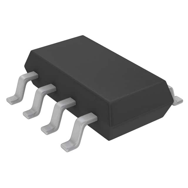
LTC2633AHTS8-LX12#TRMPBF
Product Overview
Category
LTC2633AHTS8-LX12#TRMPBF belongs to the category of digital-to-analog converters (DACs).
Use
This product is used to convert digital signals into analog signals, making it suitable for applications that require precise and accurate analog voltage outputs.
Characteristics
- High resolution: The LTC2633AHTS8-LX12#TRMPBF offers a resolution of 12 bits, ensuring fine-grained control over the analog output.
- Low power consumption: This DAC operates at low power levels, making it suitable for battery-powered devices or energy-efficient applications.
- Small package size: The LTC2633AHTS8-LX12#TRMPBF comes in a compact TSOT-8 package, allowing for space-saving integration into various electronic systems.
- Wide voltage range: It supports a wide supply voltage range, enabling compatibility with different power sources.
- Fast settling time: The DAC provides fast settling times, ensuring quick response and accurate output voltages.
Package and Quantity
The LTC2633AHTS8-LX12#TRMPBF is available in a TSOT-8 package. Each package contains one unit of the DAC.
Specifications
- Resolution: 12 bits
- Supply Voltage Range: 2.7V to 5.5V
- Output Voltage Range: 0V to Vref
- Operating Temperature Range: -40°C to +85°C
- Interface: SPI-compatible serial interface
Pin Configuration
The LTC2633AHTS8-LX12#TRMPBF has the following pin configuration:
┌───┬───┬───┬───┐
   │ VDD │ SDA │ SCL │ GND │
   └───┴───┴───┴───┘
- VDD: Power supply pin
- SDA: Serial data input pin
- SCL: Serial clock input pin
- GND: Ground pin
Functional Features
- High accuracy: The LTC2633AHTS8-LX12#TRMPBF offers excellent linearity and low integral non-linearity, ensuring accurate analog output voltages.
- Programmable output: It allows users to set the desired output voltage through the serial interface, providing flexibility in various applications.
- Internal reference: This DAC includes an internal reference voltage source, eliminating the need for an external reference component.
- Daisy-chain capability: Multiple LTC2633AHTS8-LX12#TRMPBF devices can be connected in a daisy-chain configuration, simplifying system design.
Advantages and Disadvantages
Advantages
- High resolution for precise analog voltage outputs.
- Low power consumption, suitable for energy-efficient applications.
- Compact package size for space-saving integration.
- Wide voltage range compatibility.
- Fast settling time for quick response.
Disadvantages
- Limited resolution compared to higher-end DACs.
- Single-channel output, not suitable for multi-channel applications without additional components.
Working Principles
The LTC2633AHTS8-LX12#TRMPBF operates based on the principle of digital-to-analog conversion. It receives digital input data through the serial interface and converts it into corresponding analog voltages. The internal circuitry ensures accurate conversion by utilizing a reference voltage and precise control mechanisms.
Detailed Application Field Plans
The LTC2633AHTS8-LX12#TRMPBF finds applications in various fields, including:
- Industrial automation: Precise analog voltage outputs are required for controlling motors, valves, and other industrial equipment.
- Test and measurement: The DAC is used in instrumentation applications that require accurate analog signals for testing and calibration purposes.
- Audio systems: It can be utilized in audio devices to generate high-quality analog audio signals.
- Communication systems: The DAC plays a crucial role in generating analog signals for modulation and demodulation processes.
Detailed and Complete Alternative Models
- LTC2633AHTS8-LX10#TRMPBF: Similar to LTC2633AHTS8-LX12#TRMPBF but with a 10-bit resolution.
- LTC2633AHTS8-LX14#TRMPBF: Similar to LTC2633AHTS8-LX12#TRMPBF but with a 14-bit resolution.
- LTC2633AHTS8-LX16#TRMPBF: Similar to LTC2633AHTS8-LX12#TRMPBF but with a 16-bit resolution.
These alternative models provide different resolution options to suit specific application requirements.
In conclusion, the LTC2633AHTS8-LX12#TRMPBF is a
قم بإدراج 10 أسئلة وإجابات شائعة تتعلق بتطبيق LTC2633AHTS8-LX12#TRMPBF في الحلول التقنية
Sure! Here are 10 common questions and answers related to the application of LTC2633AHTS8-LX12#TRMPBF in technical solutions:
Q: What is LTC2633AHTS8-LX12#TRMPBF? A: LTC2633AHTS8-LX12#TRMPBF is a specific model of digital-to-analog converter (DAC) manufactured by Linear Technology (now part of Analog Devices). It is designed for precision voltage output applications.
Q: What is the purpose of LTC2633AHTS8-LX12#TRMPBF? A: The purpose of LTC2633AHTS8-LX12#TRMPBF is to convert digital signals into analog voltages with high accuracy and resolution, making it suitable for various applications such as industrial control systems, instrumentation, and communication equipment.
Q: What is the resolution of LTC2633AHTS8-LX12#TRMPBF? A: LTC2633AHTS8-LX12#TRMPBF has a resolution of 12 bits, meaning it can provide 4096 discrete voltage levels between its reference voltage range.
Q: What is the supply voltage range for LTC2633AHTS8-LX12#TRMPBF? A: The supply voltage range for LTC2633AHTS8-LX12#TRMPBF is typically between 2.7V and 5.5V.
Q: How does LTC2633AHTS8-LX12#TRMPBF communicate with a microcontroller or other digital devices? A: LTC2633AHTS8-LX12#TRMPBF supports various serial communication interfaces such as I2C and SPI, allowing easy integration with microcontrollers and other digital devices.
Q: Can LTC2633AHTS8-LX12#TRMPBF operate in both single-ended and differential output modes? A: Yes, LTC2633AHTS8-LX12#TRMPBF can operate in both single-ended and differential output modes, providing flexibility in different application scenarios.
Q: What is the settling time of LTC2633AHTS8-LX12#TRMPBF? A: The settling time of LTC2633AHTS8-LX12#TRMPBF is typically around 10µs, ensuring fast and accurate voltage outputs.
Q: Does LTC2633AHTS8-LX12#TRMPBF have an internal reference voltage or does it require an external reference? A: LTC2633AHTS8-LX12#TRMPBF requires an external reference voltage for its operation. It does not have an internal reference.
Q: Is LTC2633AHTS8-LX12#TRMPBF available in different package options? A: Yes, LTC2633AHTS8-LX12#TRMPBF is available in various package options, including the HTSOP-8 package.
Q: Are there any evaluation boards or development kits available for LTC2633AHTS8-LX12#TRMPBF? A: Yes, Analog Devices provides evaluation boards and development kits specifically designed for LTC2633AHTS8-LX12#TRMPBF, which can help with prototyping and testing in different applications.
Please note that the answers provided here are general and may vary depending on the specific datasheet and documentation provided by the manufacturer.


