

MAX5113GTJ+ - English Editing Encyclopedia Entry
Product Overview
Category
MAX5113GTJ+ belongs to the category of integrated circuits (ICs).
Use
This product is commonly used in electronic devices for digital-to-analog conversion.
Characteristics
- High precision and accuracy
- Low power consumption
- Wide operating voltage range
- Compact size
Package
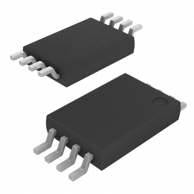
MAX5113GTJ+ is available in a small form factor package, typically a 32-pin TQFN (Thin Quad Flat No-Lead) package.
Essence
The essence of MAX5113GTJ+ lies in its ability to convert digital signals into analog voltages with high precision and efficiency.
Packaging/Quantity
This product is usually packaged in reels or tubes, with a typical quantity of 250 units per reel/tube.
Specifications
- Resolution: 12 bits
- Operating Voltage Range: 2.7V to 5.5V
- Output Voltage Range: 0V to Vref
- Total Unadjusted Error: ±1 LSB (Least Significant Bit)
- Power Consumption: 0.5mW (typical)
Detailed Pin Configuration
The MAX5113GTJ+ has a total of 32 pins. The pin configuration is as follows:
- VDD - Power supply input
- GND - Ground reference
- DIN0 - Digital input bit 0
- DIN1 - Digital input bit 1
- DIN2 - Digital input bit 2
- DIN3 - Digital input bit 3
- DIN4 - Digital input bit 4
- DIN5 - Digital input bit 5
- DIN6 - Digital input bit 6
- DIN7 - Digital input bit 7
- DIN8 - Digital input bit 8
- DIN9 - Digital input bit 9
- DIN10 - Digital input bit 10
- DIN11 - Digital input bit 11
- CS - Chip select input
- SCLK - Serial clock input
- LDAC - Load DAC input
- REFOUT - Reference voltage output
- VREF - Reference voltage input
- AGND - Analog ground reference
- OUTA - Analog output A
- OUTB - Analog output B
- OUTC - Analog output C
- OUTD - Analog output D
- OUTE - Analog output E
- OUTF - Analog output F
- OUTG - Analog output G
- OUTH - Analog output H
- NC - No connection
- NC - No connection
- NC - No connection
- NC - No connection
Functional Features
- High-resolution digital-to-analog conversion
- Serial interface for easy integration with microcontrollers
- Low power consumption for energy-efficient applications
- Internal voltage reference for accurate conversion
- Multiple analog outputs for versatile usage
Advantages and Disadvantages
Advantages
- High precision and accuracy in digital-to-analog conversion
- Wide operating voltage range allows compatibility with various systems
- Compact size enables space-saving designs
- Low power consumption for energy-efficient operation
Disadvantages
- Limited number of analog outputs may restrict certain applications
- Higher cost compared to lower-resolution DACs
Working Principles
MAX5113GTJ+ utilizes a combination of digital logic and analog circuitry to convert digital signals into corresponding analog voltages. The digital input bits control the output voltage level, which is generated using an internal voltage reference. The chip select input and serial clock input facilitate the communication between the device and the controlling microcontroller.
Detailed Application Field Plans
MAX5113GTJ+ finds applications in various fields, including:
- Audio equipment: Used for digital-to-analog conversion in audio amplifiers and music players.
- Industrial automation: Enables precise control of analog signals in industrial machinery and systems.
- Instrumentation: Provides accurate voltage generation for measurement and testing equipment.
- Communication systems: Used in wireless transceivers and base stations for signal modulation.
Detailed and Complete Alternative Models
- MAX5114GTJ+
- MAX5115GTJ+
- MAX5116GTJ+
- MAX5117GTJ+
These alternative models offer similar functionality and specifications to the MAX5113GTJ+, providing options for different system requirements.
In conclusion, the MAX5113GTJ+ is a high-precision digital-to-analog converter with a wide operating voltage range and compact size. It offers multiple analog outputs and low power consumption, making it suitable for various applications in audio equipment, industrial automation, instrumentation, and communication systems. While it has limitations in terms of the number of analog outputs and cost, there are alternative models available to cater to different needs.
قم بإدراج 10 أسئلة وإجابات شائعة تتعلق بتطبيق MAX5113GTJ+ في الحلول التقنية
Sure! Here are 10 common questions and answers related to the application of MAX5113GTJ+ in technical solutions:
Q: What is the MAX5113GTJ+? A: The MAX5113GTJ+ is a digital-to-analog converter (DAC) IC that converts digital signals into analog voltages.
Q: What is the voltage range of the MAX5113GTJ+? A: The MAX5113GTJ+ has a voltage range of 0V to VREF, where VREF is the reference voltage supplied to the DAC.
Q: How many bits does the MAX5113GTJ+ have? A: The MAX5113GTJ+ is a 12-bit DAC, meaning it can convert digital signals into 4096 different analog voltage levels.
Q: What is the supply voltage range for the MAX5113GTJ+? A: The supply voltage range for the MAX5113GTJ+ is typically between 2.7V and 5.5V.
Q: Can the MAX5113GTJ+ be used in both single-ended and differential output configurations? A: Yes, the MAX5113GTJ+ can be used in both single-ended and differential output configurations, depending on the application requirements.
Q: What is the typical settling time of the MAX5113GTJ+? A: The typical settling time of the MAX5113GTJ+ is around 10µs, which refers to the time it takes for the output voltage to reach within a specified error band after a change in the input code.
Q: Does the MAX5113GTJ+ have an internal reference voltage? A: No, the MAX5113GTJ+ does not have an internal reference voltage. An external reference voltage must be supplied to the VREF pin.
Q: Can the MAX5113GTJ+ operate in a low-power mode? A: Yes, the MAX5113GTJ+ has a low-power mode that can be enabled to reduce power consumption when the DAC is not actively being used.
Q: What is the output impedance of the MAX5113GTJ+? A: The output impedance of the MAX5113GTJ+ is typically around 0.5Ω, which means it can drive moderate loads without significant voltage drop.
Q: Is the MAX5113GTJ+ suitable for precision applications? A: Yes, the MAX5113GTJ+ is suitable for precision applications as it offers good linearity, low integral nonlinearity (INL), and low differential nonlinearity (DNL) characteristics.
Please note that these answers are general and may vary depending on the specific datasheet and application requirements.