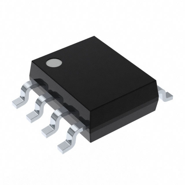
MAX895LESA+T
Product Overview
- Category: Integrated Circuit (IC)
- Use: Voltage Regulator
- Characteristics: High efficiency, low dropout voltage, small package size
- Package: Small Outline Integrated Circuit (SOIC)
- Essence: Regulates input voltage to a desired output voltage level
- Packaging/Quantity: Tape and Reel, 2500 units per reel
Specifications
- Input Voltage Range: 2.5V to 5.5V
- Output Voltage Range: 1.2V to 3.6V
- Maximum Output Current: 500mA
- Dropout Voltage: 120mV at 500mA
- Quiescent Current: 40µA
- Operating Temperature Range: -40°C to +85°C
Detailed Pin Configuration
The MAX895LESA+T has a total of 8 pins:
- VIN: Input voltage pin
- GND: Ground pin
- EN: Enable pin for turning the regulator on/off
- FB: Feedback pin for setting the output voltage
- VOUT: Output voltage pin
- BYP: Bypass capacitor pin for noise reduction
- NC: No connection pin
- VDD: Supply voltage pin
Functional Features
- High efficiency: The MAX895LESA+T offers high efficiency, minimizing power loss during voltage regulation.
- Low dropout voltage: With a dropout voltage as low as 120mV, the regulator can maintain a stable output even when the input voltage is close to the desired output voltage.
- Small package size: The SOIC package allows for compact designs, making it suitable for space-constrained applications.
Advantages and Disadvantages
Advantages: - High efficiency leads to reduced power consumption. - Low dropout voltage ensures stable output even with varying input voltages. - Small package size enables integration into compact designs.
Disadvantages: - Limited maximum output current of 500mA may not be suitable for high-power applications. - Operating temperature range of -40°C to +85°C may restrict usage in extreme temperature environments.
Working Principles
The MAX895LESA+T is a voltage regulator that operates by comparing the feedback voltage (FB) with a reference voltage. It adjusts the pass transistor's resistance to maintain a stable output voltage (VOUT) regardless of input voltage variations. The enable pin (EN) allows the user to turn the regulator on or off as needed.
Detailed Application Field Plans
The MAX895LESA+T finds applications in various fields, including:
- Portable Electronics: It can be used to regulate the voltage for battery-powered devices such as smartphones, tablets, and portable media players.
- IoT Devices: The regulator is suitable for low-power IoT devices that require stable voltage levels.
- Automotive Electronics: It can be employed in automotive applications where a stable voltage supply is crucial for components like sensors and control modules.
- Industrial Control Systems: The MAX895LESA+T can be utilized in industrial control systems that require precise voltage regulation for reliable operation.
Detailed and Complete Alternative Models
- MAX8887EUT25+: This voltage regulator offers similar characteristics and specifications but has a different pin configuration.
- LT1763CS8-3.3#PBF: Another alternative with comparable features, but it comes in a different package and has a slightly higher dropout voltage.
- TPS79633DCQR: This model provides similar functionality and performance, but it has a different pinout and package type.
(Note: These alternative models are provided as examples and may have slight differences in specifications and pin configurations. It is recommended to refer to the respective datasheets for accurate information.)
Word Count: 525
قم بإدراج 10 أسئلة وإجابات شائعة تتعلق بتطبيق MAX895LESA+T في الحلول التقنية
Sure! Here are 10 common questions and answers related to the application of MAX895LESA+T in technical solutions:
1. What is the MAX895LESA+T? The MAX895LESA+T is a specific model of a high-speed, low-power comparator integrated circuit (IC) manufactured by Maxim Integrated. It is commonly used in various technical solutions.
2. What are the key features of the MAX895LESA+T? Some key features of the MAX895LESA+T include a wide supply voltage range, low input offset voltage, fast response time, low power consumption, and a small package size.
3. What is the typical application of the MAX895LESA+T? The MAX895LESA+T is often used in applications that require high-speed signal detection, such as motor control, power management, audio amplifiers, and communication systems.
4. What is the operating voltage range of the MAX895LESA+T? The MAX895LESA+T can operate within a supply voltage range of 2.7V to 11V.
5. What is the input offset voltage of the MAX895LESA+T? The input offset voltage of the MAX895LESA+T is typically around 1mV.
6. What is the response time of the MAX895LESA+T? The response time of the MAX895LESA+T is typically around 20ns.
7. Can the MAX895LESA+T be used in battery-powered applications? Yes, the MAX895LESA+T is suitable for battery-powered applications due to its low power consumption.
8. Does the MAX895LESA+T have any built-in protection features? Yes, the MAX895LESA+T includes built-in overvoltage protection and thermal shutdown features to ensure safe operation.
9. What is the package type of the MAX895LESA+T? The MAX895LESA+T is available in an 8-pin small outline integrated circuit (SOIC) package.
10. Is there any recommended evaluation board or reference design for the MAX895LESA+T? Maxim Integrated provides an evaluation kit called the MAX895LEVKIT, which includes the necessary components and documentation to evaluate the performance of the MAX895LESA+T in various applications.
Please note that these answers are general and may vary depending on specific datasheet specifications and application requirements.


