

AT17LV040-10TQC
Product Overview
Category
AT17LV040-10TQC belongs to the category of programmable logic devices (PLDs).
Use
It is commonly used in digital circuit design and implementation.
Characteristics
- Programmable: The device can be configured to perform specific functions.
- Non-volatile: The programmed configuration remains even when power is removed.
- High-speed operation: Capable of operating at a clock frequency of up to 10 MHz.
Package
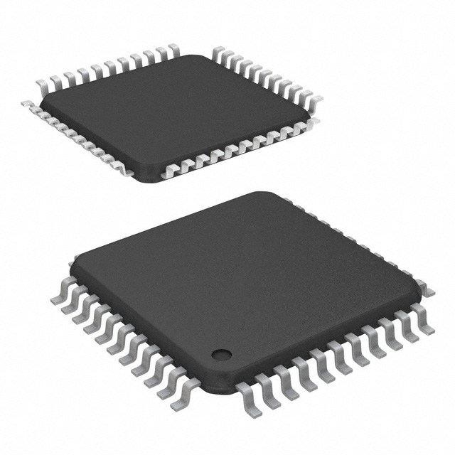
AT17LV040-10TQC comes in a small form factor package, typically a 32-pin quad flat pack (QFP).
Essence
The essence of AT17LV040-10TQC lies in its ability to provide flexible and reconfigurable logic functions for various applications.
Packaging/Quantity
The device is usually packaged in reels or tubes, with each reel or tube containing a specific quantity of AT17LV040-10TQC chips.
Specifications
- Operating Voltage: 3.3V
- Maximum Clock Frequency: 10 MHz
- Number of Logic Cells: 4,000
- Number of Input/Output Pins: 32
- Programming Technology: Flash-based
Detailed Pin Configuration
- VCC - Power supply voltage
- GND - Ground reference
- OE - Output enable
- CE - Chip enable
- A0-A7 - Address inputs
- I/O0-I/O31 - Bidirectional input/output pins
- WE - Write enable
- RESET - Reset input
- CLK - Clock input
(Note: This is a simplified pin configuration. Please refer to the datasheet for a complete pinout diagram.)
Functional Features
- In-system programmability: Allows for on-the-fly reconfiguration of the device without removing it from the circuit.
- High logic capacity: Provides a large number of logic cells for complex digital designs.
- Flexible I/O configuration: Supports bidirectional input/output pins for versatile interfacing with other devices.
- Flash-based programming: Enables easy and quick reprogramming of the device.
Advantages
- Versatility: AT17LV040-10TQC can be used in a wide range of applications due to its programmability.
- Cost-effective: Eliminates the need for multiple fixed-function chips, reducing overall system cost.
- Time-saving: In-system programmability allows for faster prototyping and design iterations.
Disadvantages
- Limited logic capacity: May not be suitable for extremely complex designs that require a higher number of logic cells.
- Power consumption: The device consumes power even when not actively performing any operations.
Working Principles
AT17LV040-10TQC utilizes flash memory technology to store the programmed configuration. When powered on, the device loads the configuration into its internal logic cells, which then determine the behavior of the circuit. The device can be reprogrammed by applying specific voltage levels to the programming pins.
Detailed Application Field Plans
AT17LV040-10TQC finds applications in various fields, including: 1. Industrial automation 2. Consumer electronics 3. Automotive systems 4. Telecommunications 5. Medical equipment
In industrial automation, it can be used for control and monitoring purposes. In consumer electronics, it can enable flexible functionality in devices such as gaming consoles and home appliances. In automotive systems, it can be utilized for engine control units and advanced driver-assistance systems. In telecommunications, it can aid in network routing and switching. In medical equipment, it can contribute to patient monitoring and diagnostic devices.
Detailed and Complete Alternative Models
- AT17LV010-10TQC: A similar device with half the logic capacity (2,000 logic cells).
- AT17LV020-10TQC: A similar device with double the logic capacity (8,000 logic cells).
- AT17LV040A-10TQC: An enhanced version with additional features and improved performance.
(Note: The above alternative models are suggestions. Please refer to the manufacturer's documentation for a complete list of alternative models.)
In conclusion, AT17LV040-10TQC is a versatile programmable logic device that offers flexibility, reconfigurability, and high-speed operation. It finds applications in various fields and can be an efficient solution for digital circuit design and implementation.
قم بإدراج 10 أسئلة وإجابات شائعة تتعلق بتطبيق AT17LV040-10TQC في الحلول التقنية
Sure! Here are 10 common questions and answers related to the application of AT17LV040-10TQC in technical solutions:
Q: What is the AT17LV040-10TQC? A: The AT17LV040-10TQC is a 4-megabit (512K x 8) low-voltage, high-speed CMOS flash memory device.
Q: What is the operating voltage range for the AT17LV040-10TQC? A: The AT17LV040-10TQC operates at a voltage range of 2.7V to 3.6V.
Q: What is the maximum clock frequency supported by the AT17LV040-10TQC? A: The AT17LV040-10TQC supports a maximum clock frequency of 33 MHz.
Q: Can the AT17LV040-10TQC be used in automotive applications? A: Yes, the AT17LV040-10TQC is suitable for use in automotive applications as it meets the necessary requirements.
Q: What is the typical access time of the AT17LV040-10TQC? A: The typical access time of the AT17LV040-10TQC is 100 ns.
Q: Does the AT17LV040-10TQC support sector erase operation? A: Yes, the AT17LV040-10TQC supports sector erase operation, allowing specific sectors to be erased.
Q: Can the AT17LV040-10TQC be reprogrammed multiple times? A: Yes, the AT17LV040-10TQC can be reprogrammed multiple times, making it suitable for applications that require frequent updates.
Q: What is the endurance rating of the AT17LV040-10TQC? A: The AT17LV040-10TQC has an endurance rating of 100,000 erase/write cycles per sector.
Q: Does the AT17LV040-10TQC have any security features? A: Yes, the AT17LV040-10TQC provides a software write protection feature to prevent unauthorized modifications.
Q: What package options are available for the AT17LV040-10TQC? A: The AT17LV040-10TQC is available in various package options, including 32-lead TQFP and 32-ball CSP.