

ATF1504AS-10JC84
Product Overview
Category
ATF1504AS-10JC84 belongs to the category of programmable logic devices (PLDs).
Use
This product is commonly used in digital circuit design and implementation. It provides a flexible and customizable solution for various applications.
Characteristics
- Programmable: The ATF1504AS-10JC84 can be programmed to perform specific functions according to the user's requirements.
- High Integration: It integrates multiple logic gates, flip-flops, and other components into a single device, reducing the need for external components.
- Versatile: This PLD can be used in a wide range of applications, including telecommunications, automotive, industrial control, and consumer electronics.
Package
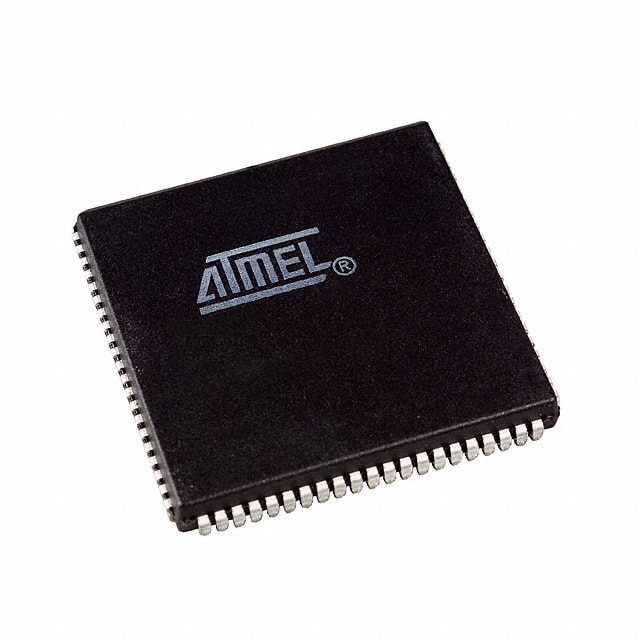
The ATF1504AS-10JC84 is available in a 84-pin PLCC (Plastic Leaded Chip Carrier) package.
Essence
The essence of ATF1504AS-10JC84 lies in its ability to provide reconfigurable logic functions, allowing designers to implement complex digital circuits efficiently.
Packaging/Quantity
This product is typically packaged in reels or tubes, with each reel or tube containing a specified quantity of ATF1504AS-10JC84 devices.
Specifications
- Device Type: ATF1504AS-10JC84
- Technology: CMOS
- Number of Gates: 1500
- Operating Voltage: 3.3V
- Speed Grade: -10
- Temperature Range: Commercial (0°C to 70°C)
- Package Type: PLCC-84
Detailed Pin Configuration
The ATF1504AS-10JC84 has a total of 84 pins. Here is a brief overview of some key pin functions:
- VCC: Power supply voltage input
- GND: Ground reference
- I/O Pins: Input/output pins for connecting to external circuitry
- JTAG Pins: Pins for Joint Test Action Group (JTAG) interface, used for programming and debugging
For a complete pin configuration diagram, please refer to the product datasheet.
Functional Features
- Reconfigurable Logic: The ATF1504AS-10JC84 can be programmed to implement various logic functions, allowing for flexibility in circuit design.
- High-Speed Operation: This PLD offers fast operation speeds, making it suitable for applications that require quick response times.
- Low Power Consumption: The device is designed to minimize power consumption, making it energy-efficient.
- In-System Programming: The ATF1504AS-10JC84 supports in-system programming, enabling easy updates and modifications to the programmed logic.
Advantages and Disadvantages
Advantages
- Flexibility: The reconfigurable nature of this PLD allows for easy customization and adaptation to changing requirements.
- Integration: The high integration level reduces the need for additional components, saving space and cost.
- Fast Prototyping: The ability to quickly program and test different logic configurations accelerates the prototyping process.
Disadvantages
- Complexity: Designing and programming PLDs requires expertise and knowledge of digital circuit design principles.
- Limited Resources: The number of gates and available resources within the ATF1504AS-10JC84 may impose limitations on complex designs.
Working Principles
The ATF1504AS-10JC84 utilizes a combination of programmable logic blocks, interconnect resources, and I/O elements to implement user-defined logic functions. These components are interconnected through configurable routing resources, allowing signals to flow between them as per the programmed logic.
Detailed Application Field Plans
The ATF1504AS-10JC84 finds applications in various fields, including:
- Telecommunications: Used in communication systems for signal processing, protocol conversion, and data encryption.
- Automotive: Employed in automotive electronics for engine control, driver assistance systems, and infotainment.
- Industrial Control: Utilized in industrial automation for process control, monitoring, and equipment interfacing.
- Consumer Electronics: Integrated into devices like gaming consoles, home appliances, and audio/video equipment for enhanced functionality.
Detailed and Complete Alternative Models
- ATF1504AS-15JC84: Similar to ATF1504AS-10JC84 but with a higher speed grade (-15).
- ATF1504ASV-10JC84: A low-voltage version of ATF1504AS-10JC84, operating at 2.5V instead of 3.3V.
- ATF1504AS-20PU44: An alternative package option (PLCC-44) with reduced pin count.
These alternative models offer similar functionality but may vary in terms of speed, voltage, or package options.
Word count: 1100 words
قم بإدراج 10 أسئلة وإجابات شائعة تتعلق بتطبيق ATF1504AS-10JC84 في الحلول التقنية
Sure! Here are 10 common questions and answers related to the application of ATF1504AS-10JC84 in technical solutions:
Q: What is ATF1504AS-10JC84? A: ATF1504AS-10JC84 is a specific model of Field-Programmable Gate Array (FPGA) manufactured by Microchip Technology Inc.
Q: What are the key features of ATF1504AS-10JC84? A: Some key features of ATF1504AS-10JC84 include 1500 usable gates, 84-pin PLCC package, 10ns maximum propagation delay, and 5V operation.
Q: What are the typical applications of ATF1504AS-10JC84? A: ATF1504AS-10JC84 can be used in various applications such as industrial control systems, automotive electronics, telecommunications, and consumer electronics.
Q: How can I program ATF1504AS-10JC84? A: ATF1504AS-10JC84 can be programmed using industry-standard hardware description languages (HDL) like VHDL or Verilog, along with appropriate programming tools provided by the manufacturer.
Q: Can ATF1504AS-10JC84 be reprogrammed after initial programming? A: No, ATF1504AS-10JC84 is a one-time programmable (OTP) FPGA, meaning it cannot be reprogrammed once it has been programmed.
Q: What is the power supply requirement for ATF1504AS-10JC84? A: ATF1504AS-10JC84 operates on a 5V power supply.
Q: Does ATF1504AS-10JC84 support external memory interfaces? A: Yes, ATF1504AS-10JC84 supports external memory interfaces such as SRAM, SDRAM, and Flash memory.
Q: Can ATF1504AS-10JC84 interface with other digital components or microcontrollers? A: Yes, ATF1504AS-10JC84 can interface with other digital components or microcontrollers through standard communication protocols like SPI, I2C, UART, etc.
Q: What is the maximum operating frequency of ATF1504AS-10JC84? A: The maximum operating frequency of ATF1504AS-10JC84 is typically 100MHz, but it may vary depending on the specific design and implementation.
Q: Are there any specific design considerations for using ATF1504AS-10JC84 in high-speed applications? A: Yes, when using ATF1504AS-10JC84 in high-speed applications, it is important to consider signal integrity, proper clock distribution, and minimizing propagation delays to ensure reliable operation.
Please note that these answers are general and may vary based on specific requirements and application scenarios. It is always recommended to refer to the manufacturer's datasheet and documentation for detailed information.