

A3P600-1FGG256I
Product Overview
Category
A3P600-1FGG256I belongs to the category of programmable logic devices (PLDs).
Use
This product is primarily used in digital circuit design and implementation. It provides a flexible and customizable solution for various applications.
Characteristics
- Programmable: The A3P600-1FGG256I can be programmed to perform specific functions based on user requirements.
- High Integration: It offers a high level of integration, allowing for complex designs to be implemented on a single device.
- Versatile: This PLD supports a wide range of applications due to its programmability.
- Low Power Consumption: The A3P600-1FGG256I is designed to operate efficiently with low power consumption.
Package
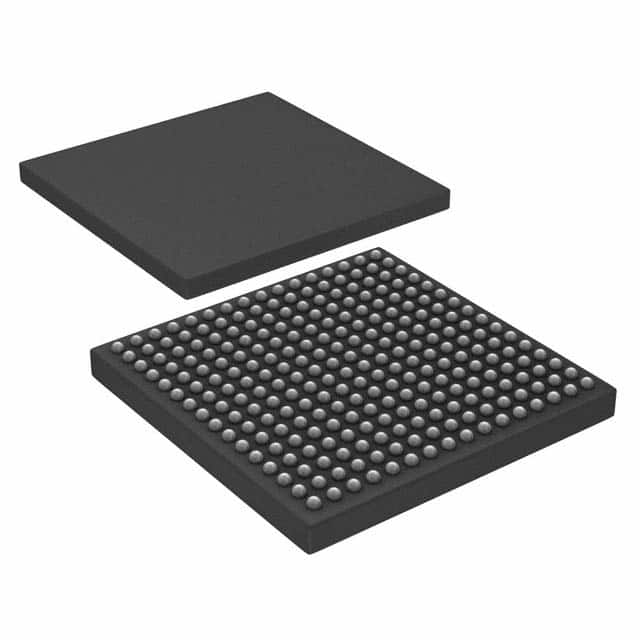
The A3P600-1FGG256I is available in a 256-pin Fine-Pitch Ball Grid Array (FBGA) package.
Essence
The essence of this product lies in its ability to provide a reconfigurable hardware platform that enables users to implement custom digital circuits.
Packaging/Quantity
The A3P600-1FGG256I is typically packaged individually and is available in various quantities depending on customer requirements.
Specifications
- Device Type: Programmable Logic Device (PLD)
- Family: A3P
- Series: 600
- Package: 256-pin FBGA
- Operating Voltage: 3.3V
- Number of Logic Elements: 600
- Number of I/O Pins: 256
- Maximum Frequency: 100 MHz
- Programmable Logic Blocks: 30
- Embedded Memory: 64 Kbits
- On-Chip PLLs: 2
- JTAG Interface: Yes
Detailed Pin Configuration
The pin configuration of the A3P600-1FGG256I is as follows:
- Pin 1: VCCIO
- Pin 2: GND
- Pin 3: JTAG_TMS
- Pin 4: JTAG_TCK
- Pin 5: JTAG_TDI
- Pin 6: JTAG_TDO
- ...
- Pin 256: VCCIO
Functional Features
The A3P600-1FGG256I offers the following functional features:
- Programmable Logic Blocks: These blocks can be configured to perform various logic functions.
- Embedded Memory: The device includes on-chip memory for storing data.
- PLLs: Two Phase-Locked Loops (PLLs) are available for clock management and synchronization.
- JTAG Interface: The Joint Test Action Group (JTAG) interface allows for programming and debugging of the device.
Advantages and Disadvantages
Advantages
- Flexibility: The A3P600-1FGG256I provides flexibility in designing and implementing digital circuits.
- Integration: It offers a high level of integration, reducing the need for additional components.
- Customizability: Users can program the device to meet specific requirements.
- Low Power Consumption: The product operates efficiently with low power consumption.
Disadvantages
- Learning Curve: Utilizing the full potential of the A3P600-1FGG256I may require a learning curve for users unfamiliar with programmable logic devices.
- Cost: PLDs can be more expensive compared to fixed-function integrated circuits for certain applications.
Working Principles
The A3P600-1FGG256I works based on the principles of reconfigurable hardware. It consists of programmable logic blocks that can be interconnected to create custom digital circuits. These logic blocks can be programmed using Hardware Description Languages (HDLs) such as VHDL or Verilog. The resulting configuration is stored in the device's memory and executed based on input signals.
Detailed Application Field Plans
The A3P600-1FGG256I finds applications in various fields, including:
- Communications: It can be used in networking equipment, routers, and switches.
- Industrial Automation: The PLD can be employed in control systems and programmable logic controllers (PLCs).
- Consumer Electronics: It can be utilized in smart home devices, gaming consoles, and multimedia systems.
- Automotive: The A3P600-1FGG256I can be integrated into automotive electronics for functions like engine control and driver assistance systems.
- Medical Devices: It finds application in medical imaging equipment, patient monitoring systems, and laboratory instruments.
Detailed and Complete Alternative Models
Some alternative models to the A3P600-1FGG256I include:
- A3P030-VQG100: This model offers a smaller logic capacity but is more cost-effective for simpler designs.
- A3P1000-FGG144: With a higher logic capacity, this model is suitable for more complex applications.
قم بإدراج 10 أسئلة وإجابات شائعة تتعلق بتطبيق A3P600-1FGG256I في الحلول التقنية
Sure! Here are 10 common questions and answers related to the application of A3P600-1FGG256I in technical solutions:
Q1: What is A3P600-1FGG256I? A1: A3P600-1FGG256I is a specific model of FPGA (Field-Programmable Gate Array) manufactured by Microsemi Corporation.
Q2: What is an FPGA? A2: FPGA stands for Field-Programmable Gate Array. It is a type of integrated circuit that can be programmed or reconfigured after manufacturing to perform specific functions.
Q3: What are the key features of A3P600-1FGG256I? A3: Some key features of A3P600-1FGG256I include 600,000 system gates, 256-pin FineLine BGA package, and support for various I/O standards.
Q4: What are the typical applications of A3P600-1FGG256I? A4: A3P600-1FGG256I can be used in a wide range of applications such as industrial automation, telecommunications, automotive electronics, medical devices, and more.
Q5: How can A3P600-1FGG256I be programmed? A5: A3P600-1FGG256I can be programmed using hardware description languages (HDLs) like VHDL or Verilog, which describe the desired functionality of the FPGA.
Q6: Can A3P600-1FGG256I be used for real-time signal processing? A6: Yes, A3P600-1FGG256I can be used for real-time signal processing tasks due to its high-speed performance and programmability.
Q7: Does A3P600-1FGG256I support external memory interfaces? A7: Yes, A3P600-1FGG256I supports various external memory interfaces like DDR, SDRAM, and Flash memory.
Q8: Can A3P600-1FGG256I interface with other devices or microcontrollers? A8: Yes, A3P600-1FGG256I can interface with other devices or microcontrollers through its I/O pins, allowing for seamless integration into larger systems.
Q9: What development tools are available for programming A3P600-1FGG256I? A9: Microsemi provides development tools like Libero SoC Design Suite, which includes a complete design flow for programming and debugging the FPGA.
Q10: Are there any application notes or reference designs available for A3P600-1FGG256I? A10: Yes, Microsemi provides application notes and reference designs that can help users get started with implementing A3P600-1FGG256I in their technical solutions.
Please note that the specific details and answers may vary depending on the manufacturer's documentation and the user's requirements.