

A40MX02-1PLG68
Product Overview
Category
The A40MX02-1PLG68 belongs to the category of programmable logic devices (PLDs).
Use
This product is primarily used in digital circuit design and implementation. It provides a flexible and customizable solution for various applications that require logic functions.
Characteristics
- Programmable: The A40MX02-1PLG68 can be programmed to perform specific logic functions based on the user's requirements.
- Versatile: It supports a wide range of applications due to its programmability.
- High-density: This PLD offers a high number of logic gates, allowing for complex designs.
- Low power consumption: The A40MX02-1PLG68 is designed to operate efficiently with minimal power consumption.
Package
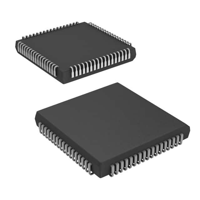
The A40MX02-1PLG68 is available in a 68-pin plastic leaded chip carrier (PLCC) package.
Essence
The essence of the A40MX02-1PLG68 lies in its ability to provide a reconfigurable logic solution, enabling designers to implement custom logic functions without the need for dedicated hardware.
Packaging/Quantity
This product is typically packaged individually and is available in various quantities depending on the manufacturer's specifications.
Specifications
- Logic Gates: The A40MX02-1PLG68 offers a total of 2,000 logic gates.
- I/O Pins: It provides 68 input/output pins for interfacing with external devices.
- Operating Voltage: The recommended operating voltage range is between 3.0V and 3.6V.
- Speed Grade: This PLD is available in different speed grades, ranging from standard to high-performance options.
Detailed Pin Configuration
The A40MX02-1PLG68 features the following pin configuration:
- Pin 1: VCCIO
- Pin 2: GND
- Pin 3: IO1
- Pin 4: IO2
- ...
- Pin 68: IO68
Functional Features
- Reconfigurability: The A40MX02-1PLG68 can be reprogrammed multiple times, allowing for design changes and updates.
- In-system programming: It supports in-system programming, enabling the device to be programmed while in operation.
- JTAG Interface: This PLD includes a Joint Test Action Group (JTAG) interface for debugging and testing purposes.
Advantages and Disadvantages
Advantages
- Flexibility: The A40MX02-1PLG68 offers flexibility in designing complex logic functions.
- Cost-effective: By eliminating the need for dedicated hardware, this PLD reduces overall costs.
- Time-saving: Design iterations can be quickly implemented through reprogramming, saving time in the development process.
Disadvantages
- Learning curve: Utilizing programmable logic devices requires knowledge of hardware description languages and digital circuit design principles.
- Limited resources: The number of available logic gates and I/O pins may restrict the complexity of designs that can be implemented.
Working Principles
The A40MX02-1PLG68 operates based on the principles of field-programmable gate arrays (FPGAs). It consists of an array of configurable logic blocks (CLBs) interconnected through programmable interconnects. These CLBs can be programmed to implement various logic functions, allowing for the creation of custom digital circuits.
Detailed Application Field Plans
The A40MX02-1PLG68 finds applications in various fields, including:
- Communications: It can be used in networking equipment, such as routers and switches, to implement custom logic functions for data processing and routing.
- Industrial Automation: This PLD is suitable for controlling and monitoring systems in industrial automation, enabling the implementation of specific logic functions tailored to the application requirements.
- Consumer Electronics: It can be utilized in consumer electronic devices, such as gaming consoles and multimedia systems, to implement custom logic for enhanced functionality.
Detailed and Complete Alternative Models
- A40MX04-1PLG68: This model offers double the number of logic gates compared to the A40MX02-1PLG68, providing increased design flexibility.
- A40MX08-1PLG68: With four times the logic gates of the A40MX02-1PLG68, this model is suitable for more complex digital circuit designs.
- A40MX16-1PLG68: This high-density PLD provides sixteen times the logic gates of the A40MX02-1PLG68, catering to demanding applications requiring extensive logic functions.
Note: The above alternative models are suggestions and may vary based on availability and specific requirements.
In conclusion, the A40MX02-1PLG68 is a versatile programmable logic device that offers flexibility, cost-effectiveness, and time-saving benefits. Its reconfig
قم بإدراج 10 أسئلة وإجابات شائعة تتعلق بتطبيق A40MX02-1PLG68 في الحلول التقنية
Sure! Here are 10 common questions and answers related to the application of A40MX02-1PLG68 in technical solutions:
Q1: What is A40MX02-1PLG68? A1: A40MX02-1PLG68 is a specific model of field-programmable gate array (FPGA) manufactured by Microsemi Corporation.
Q2: What are the key features of A40MX02-1PLG68? A2: Some key features of A40MX02-1PLG68 include 40,000 usable gates, 2,048 macrocells, 68-pin PLCC package, and support for various I/O standards.
Q3: What are the typical applications of A40MX02-1PLG68? A3: A40MX02-1PLG68 is commonly used in applications such as telecommunications, industrial automation, automotive electronics, and aerospace systems.
Q4: How can A40MX02-1PLG68 be programmed? A4: A40MX02-1PLG68 can be programmed using hardware description languages (HDLs) like VHDL or Verilog, which are then synthesized into configuration files that can be loaded onto the FPGA.
Q5: Can A40MX02-1PLG68 be reprogrammed after deployment? A5: Yes, A40MX02-1PLG68 is a reprogrammable FPGA, allowing for updates and modifications to the design even after it has been deployed in a system.
Q6: What are the power requirements for A40MX02-1PLG68? A6: The power requirements for A40MX02-1PLG68 typically range from 3.3V to 5V, depending on the specific implementation and configuration.
Q7: Does A40MX02-1PLG68 support different I/O standards? A7: Yes, A40MX02-1PLG68 supports various I/O standards such as LVCMOS, LVTTL, LVDS, and HSTL, making it versatile for interfacing with different components and systems.
Q8: Can A40MX02-1PLG68 interface with external memory devices? A8: Yes, A40MX02-1PLG68 has dedicated pins and features to interface with external memory devices like SRAM, SDRAM, or Flash memory.
Q9: What is the maximum operating frequency of A40MX02-1PLG68? A9: The maximum operating frequency of A40MX02-1PLG68 depends on the specific design and implementation, but it can typically reach frequencies in the range of tens to hundreds of megahertz.
Q10: Are there any development tools available for programming A40MX02-1PLG68? A10: Yes, Microsemi provides development tools like Libero SoC Design Suite and Designer Software that facilitate the design, simulation, synthesis, and programming of A40MX02-1PLG68 FPGAs.
Please note that the answers provided here are general and may vary depending on the specific requirements and implementation of A40MX02-1PLG68 in a technical solution.