

A54SX08-2VQ100I
Product Overview
Category
The A54SX08-2VQ100I belongs to the category of Field Programmable Gate Arrays (FPGAs).
Use
FPGAs are integrated circuits that can be programmed and reprogrammed to perform various digital functions. The A54SX08-2VQ100I is specifically designed for applications requiring high-performance logic integration.
Characteristics
- High-performance FPGA with advanced logic integration capabilities.
- Offers flexibility in designing and implementing complex digital systems.
- Can be reprogrammed multiple times, allowing for iterative development and customization.
- Provides a wide range of configurable logic blocks and input/output resources.
- Supports various communication protocols and interfaces.
- Offers high-speed data processing and low power consumption.
Package and Quantity
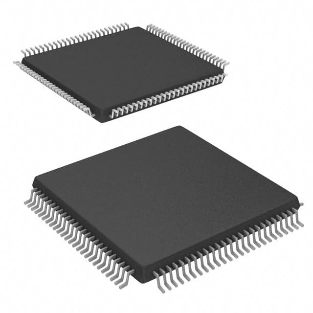
The A54SX08-2VQ100I is available in a 100-pin Very Thin Quad Flat Pack (VQFP) package. It is typically sold individually or in small quantities.
Specifications
- Logic Elements: 8,000
- Maximum User I/Os: 96
- Block RAM: 288 Kbits
- Clock Management Tiles: 4
- Maximum Frequency: 250 MHz
- Operating Voltage: 3.3V
- Package Type: VQFP
- Package Pins: 100
- Temperature Range: -40°C to +85°C
Pin Configuration
The detailed pin configuration of the A54SX08-2VQ100I can be found in the manufacturer's datasheet.
Functional Features
- Configurable logic blocks allow for the implementation of various digital functions.
- Dedicated clock management tiles enable precise timing control.
- Flexible routing resources facilitate interconnection between different logic elements.
- On-chip memory blocks provide efficient storage for data processing.
- Support for various communication protocols enables seamless integration with external devices.
- Built-in security features protect the design from unauthorized access.
Advantages and Disadvantages
Advantages
- High-performance logic integration capabilities.
- Flexibility in design and customization.
- Reprogrammable nature allows for iterative development.
- Wide range of configurable logic blocks and I/O resources.
- Support for various communication protocols.
- Low power consumption.
Disadvantages
- Relatively high cost compared to other programmable logic devices.
- Steeper learning curve for programming and utilizing the full potential of FPGAs.
- Limited availability of alternative models with similar specifications.
Working Principles
The A54SX08-2VQ100I operates based on the principles of reconfigurable digital logic. It consists of a matrix of configurable logic blocks interconnected through programmable routing resources. The device can be programmed using Hardware Description Languages (HDLs) such as VHDL or Verilog, which define the desired functionality and interconnections within the FPGA. Once programmed, the FPGA executes the specified logic functions, enabling the implementation of complex digital systems.
Application Field Plans
The A54SX08-2VQ100I finds applications in various fields, including:
- Telecommunications: Used in base stations, network routers, and switches for high-speed data processing and protocol handling.
- Industrial Automation: Employed in control systems, robotics, and machine vision applications for real-time data processing and control.
- Aerospace and Defense: Utilized in radar systems, avionics, and military-grade communication equipment for high-performance signal processing and encryption.
- Medical Devices: Integrated into medical imaging systems, patient monitoring devices, and laboratory equipment for data acquisition and processing.
- Automotive: Applied in advanced driver assistance systems (ADAS), infotainment systems, and engine control units for efficient data processing and control.
Alternative Models
While the A54SX08-2VQ100I offers unique features and specifications, alternative models with similar capabilities include:
- Xilinx Spartan-6 XC6SLX9: Offers comparable logic capacity and I/O resources.
- Altera Cyclone IV EP4CE22: Provides similar performance and flexibility in a different package.
- Lattice iCE40HX8K: A low-power FPGA with a smaller form factor suitable for portable devices.
These alternative models can be considered based on specific project requirements and availability.
Word count: 550 words
قم بإدراج 10 أسئلة وإجابات شائعة تتعلق بتطبيق A54SX08-2VQ100I في الحلول التقنية
Sure! Here are 10 common questions and answers related to the application of A54SX08-2VQ100I in technical solutions:
Question: What is the A54SX08-2VQ100I?
Answer: The A54SX08-2VQ100I is a specific model of a field-programmable gate array (FPGA) manufactured by Microsemi.Question: What are the key features of the A54SX08-2VQ100I?
Answer: Some key features of this FPGA include 8,192 logic elements, 256 I/O pins, and support for various communication protocols.Question: In what types of technical solutions can the A54SX08-2VQ100I be used?
Answer: The A54SX08-2VQ100I can be used in a wide range of applications such as telecommunications, industrial automation, aerospace, and defense.Question: How can I program the A54SX08-2VQ100I?
Answer: The A54SX08-2VQ100I can be programmed using hardware description languages (HDLs) like VHDL or Verilog, and then configured using appropriate software tools provided by Microsemi.Question: Can the A54SX08-2VQ100I be reprogrammed after deployment?
Answer: Yes, the A54SX08-2VQ100I is a reprogrammable FPGA, allowing you to modify its functionality even after it has been deployed in a system.Question: What are some advantages of using the A54SX08-2VQ100I in technical solutions?
Answer: The A54SX08-2VQ100I offers advantages such as high flexibility, low power consumption, fast processing speeds, and the ability to implement complex algorithms.Question: Are there any limitations or considerations when using the A54SX08-2VQ100I?
Answer: Some considerations include the need for expertise in FPGA programming, potential resource limitations depending on the complexity of the design, and the cost associated with FPGA development.Question: Can the A54SX08-2VQ100I interface with other components or devices?
Answer: Yes, the A54SX08-2VQ100I can interface with various components and devices through its I/O pins, allowing for seamless integration into larger systems.Question: Is technical support available for the A54SX08-2VQ100I?
Answer: Yes, Microsemi provides technical support for their FPGAs, including documentation, online resources, and direct assistance from their support team.Question: Where can I find more information about the A54SX08-2VQ100I?
Answer: You can find more detailed information about the A54SX08-2VQ100I on Microsemi's official website, including datasheets, application notes, and reference designs.