

A54SX16A-FG144I
Product Overview
Category
The A54SX16A-FG144I belongs to the category of Field-Programmable Gate Arrays (FPGAs).
Use
This FPGA is commonly used in electronic circuits for various applications, including digital signal processing, telecommunications, and embedded systems.
Characteristics
- High-performance programmable logic device
- Offers flexibility and reconfigurability
- Provides a large number of configurable logic blocks and input/output pins
- Supports complex digital designs
- Enables rapid prototyping and development of custom digital circuits
Package
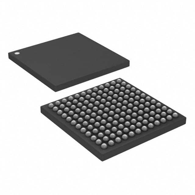
The A54SX16A-FG144I comes in a compact and durable package suitable for integration into electronic systems. The package ensures protection against environmental factors such as moisture, dust, and temperature variations.
Essence
The essence of the A54SX16A-FG144I lies in its ability to provide a customizable and versatile solution for digital circuit design. It allows designers to implement complex logic functions and adapt them as per their specific requirements.
Packaging/Quantity
The A54SX16A-FG144I is typically packaged individually and is available in varying quantities depending on the manufacturer or distributor.
Specifications
- FPGA Family: A54SX
- Logic Cells: 16,000
- Package Type: FG144
- Operating Voltage: 3.3V
- Maximum Frequency: 200 MHz
- I/O Pins: 144
- Embedded Memory: 576 Kbits
- Programmable Interconnect Points: 22,464
Detailed Pin Configuration
The A54SX16A-FG144I has a total of 144 pins, each serving a specific purpose in the overall functionality of the FPGA. The pin configuration includes input, output, and bidirectional pins, as well as dedicated pins for power supply and configuration purposes. For a detailed pin configuration diagram, please refer to the manufacturer's datasheet.
Functional Features
- High-speed performance
- Reconfigurable architecture
- Support for various I/O standards
- On-chip memory resources
- Built-in clock management circuitry
- Flexible routing and interconnect options
- Support for partial reconfiguration
Advantages and Disadvantages
Advantages
- Flexibility in design implementation
- Rapid prototyping and development
- Cost-effective compared to custom ASICs
- Shorter time-to-market
- Ability to adapt to changing requirements
Disadvantages
- Higher power consumption compared to dedicated hardware solutions
- Limited resources for complex designs
- Steeper learning curve for beginners
- Debugging and verification challenges
Working Principles
The A54SX16A-FG144I operates based on the principles of configurable logic. It consists of programmable logic blocks interconnected through a flexible routing fabric. The FPGA can be programmed using Hardware Description Languages (HDL) such as VHDL or Verilog. Upon programming, the FPGA configures its internal resources to implement the desired digital circuit functionality.
Detailed Application Field Plans
The A54SX16A-FG144I finds applications in various fields, including:
- Telecommunications: Used in base stations, network switches, and routers for signal processing and protocol handling.
- Industrial Automation: Employed in control systems, motor drives, and robotics for real-time data processing and control.
- Medical Devices: Integrated into medical imaging equipment, patient monitoring systems, and diagnostic devices for data acquisition and processing.
- Aerospace and Defense: Utilized in radar systems, avionics, and communication equipment for high-performance signal processing and encryption.
- Automotive: Incorporated into advanced driver assistance systems (ADAS), infotainment systems, and engine control units for enhanced functionality and performance.
Detailed and Complete Alternative Models
- A54SX32A-FG256I: Offers double the logic cells and I/O pins compared to A54SX16A-FG144I.
- A54SX08A-FG144I: Provides a lower-cost option with reduced logic cells and I/O pins.
- A54SX64A-FG484I: Suitable for more complex designs, offering higher logic capacity and increased I/O options.
These alternative models cater to different design requirements and can be considered based on the specific needs of the application.
Word count: 550 words
قم بإدراج 10 أسئلة وإجابات شائعة تتعلق بتطبيق A54SX16A-FG144I في الحلول التقنية
Sure! Here are 10 common questions and answers related to the application of A54SX16A-FG144I in technical solutions:
Q: What is the A54SX16A-FG144I? A: The A54SX16A-FG144I is a specific model of field-programmable gate array (FPGA) manufactured by Microsemi Corporation.
Q: What are the key features of the A54SX16A-FG144I? A: The A54SX16A-FG144I offers 54,000 system gates, 16,000 usable gates, 144-pin FineLine BGA package, and various I/O options.
Q: In what applications can the A54SX16A-FG144I be used? A: The A54SX16A-FG144I can be used in a wide range of applications such as industrial automation, telecommunications, medical devices, and automotive systems.
Q: How does the A54SX16A-FG144I differ from other FPGAs? A: The A54SX16A-FG144I stands out with its low power consumption, high reliability, and advanced security features, making it suitable for mission-critical applications.
Q: Can the A54SX16A-FG144I be programmed using industry-standard tools? A: Yes, the A54SX16A-FG144I can be programmed using popular FPGA development tools like Xilinx Vivado or Intel Quartus Prime.
Q: What kind of I/O interfaces does the A54SX16A-FG144I support? A: The A54SX16A-FG144I supports a variety of I/O standards, including LVCMOS, LVTTL, SSTL, HSTL, LVDS, and differential signaling.
Q: Is the A54SX16A-FG144I suitable for high-speed data processing? A: Yes, the A54SX16A-FG144I offers dedicated high-speed I/O pins and advanced clock management resources, making it well-suited for high-speed data processing applications.
Q: Can the A54SX16A-FG144I be used in safety-critical systems? A: Yes, the A54SX16A-FG144I supports functional safety features like error correction codes (ECC) and built-in self-test (BIST), making it suitable for safety-critical applications.
Q: Are there any development boards available for the A54SX16A-FG144I? A: Yes, Microsemi provides development boards specifically designed for the A54SX16A-FG144I, which can aid in prototyping and evaluation of the FPGA.
Q: Where can I find more information about the A54SX16A-FG144I? A: You can find detailed technical documentation, datasheets, and application notes on Microsemi's official website or by contacting their support team directly.