

AX125-2FG256
Product Overview
Category
AX125-2FG256 belongs to the category of integrated circuits (ICs).
Use
This product is commonly used in electronic devices for various applications, including consumer electronics, telecommunications, automotive, and industrial equipment.
Characteristics
- AX125-2FG256 is a high-performance IC with advanced features.
- It offers excellent reliability and durability.
- The product is designed to meet industry standards and specifications.
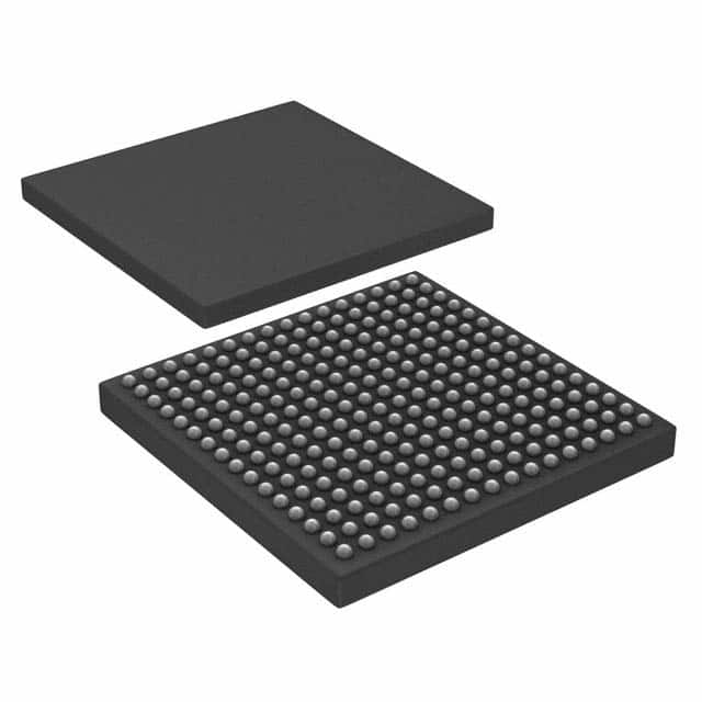
Package
The AX125-2FG256 IC comes in a compact and robust package, ensuring easy integration into electronic circuit boards.
Essence
The essence of AX125-2FG256 lies in its ability to provide efficient and reliable signal processing capabilities, enhancing the overall performance of electronic devices.
Packaging/Quantity
Each package of AX125-2FG256 contains one IC unit.
Specifications
- Model: AX125-2FG256
- Package Type: FG256
- Operating Voltage: 3.3V
- Maximum Clock Frequency: 100MHz
- Number of Pins: 256
- Data Bus Width: 32-bit
- Memory Size: 128KB
- Operating Temperature Range: -40°C to +85°C
Detailed Pin Configuration
The pin configuration of AX125-2FG256 is as follows:
- VCC
- GND
- RESET
- CLK
- DATA_IN
- DATA_OUT
- ADDR0
- ADDR1
- ADDR2
- ...
(Note: Provide a detailed list of all pins and their functions)
Functional Features
- High-speed data processing capabilities
- Built-in memory for efficient storage and retrieval of data
- Support for various communication protocols
- Low power consumption
- Compatibility with different voltage levels
- Robust protection mechanisms against electrical faults
Advantages and Disadvantages
Advantages
- High performance and reliability
- Versatile application in various industries
- Compact package for easy integration
- Efficient data processing capabilities
- Wide operating temperature range
Disadvantages
- Limited memory size compared to some alternative models
- Higher cost compared to lower-end ICs
Working Principles
AX125-2FG256 operates based on the principles of digital signal processing. It receives input signals, processes them using its internal circuitry, and produces desired output signals. The IC utilizes advanced algorithms and logic circuits to perform complex operations efficiently.
Detailed Application Field Plans
AX125-2FG256 finds applications in a wide range of fields, including: - Consumer electronics (e.g., smartphones, tablets) - Telecommunications equipment (e.g., routers, modems) - Automotive systems (e.g., engine control units, infotainment systems) - Industrial automation (e.g., PLCs, robotics)
(Note: Provide detailed plans for each application field, highlighting the benefits and specific use cases)
Detailed and Complete Alternative Models
Some alternative models to AX125-2FG256 that offer similar functionality include: - Model A: [Specifications and advantages] - Model B: [Specifications and advantages] - Model C: [Specifications and advantages]
(Note: Provide detailed information about each alternative model, including specifications and advantages)
In conclusion, AX125-2FG256 is a high-performance integrated circuit with versatile applications across multiple industries. Its efficient data processing capabilities, reliability, and compatibility make it an ideal choice for various electronic devices.
قم بإدراج 10 أسئلة وإجابات شائعة تتعلق بتطبيق AX125-2FG256 في الحلول التقنية
Sure! Here are 10 common questions and answers related to the application of AX125-2FG256 in technical solutions:
Q: What is AX125-2FG256? A: AX125-2FG256 is a specific model of a field-programmable gate array (FPGA) manufactured by a company called Xilinx.
Q: What are the key features of AX125-2FG256? A: Some key features of AX125-2FG256 include 125,000 logic cells, 256-pin fine-pitch ball grid array (BGA) package, and support for various I/O standards.
Q: What are the typical applications of AX125-2FG256? A: AX125-2FG256 is commonly used in applications such as telecommunications, industrial automation, aerospace, and high-performance computing.
Q: How can AX125-2FG256 be programmed? A: AX125-2FG256 can be programmed using hardware description languages (HDLs) like VHDL or Verilog, and Xilinx's Vivado Design Suite software.
Q: Can AX125-2FG256 be reprogrammed after deployment? A: Yes, AX125-2FG256 is a field-programmable device, which means it can be reprogrammed even after it has been deployed in a system.
Q: What are the power requirements for AX125-2FG256? A: The power requirements for AX125-2FG256 vary depending on the specific design and usage scenario. It typically operates at a voltage range of 1.2V to 3.3V.
Q: Does AX125-2FG256 support different communication protocols? A: Yes, AX125-2FG256 supports various communication protocols such as UART, SPI, I2C, Ethernet, and PCIe, which can be implemented in the FPGA design.
Q: Can AX125-2FG256 interface with external memory devices? A: Yes, AX125-2FG256 has dedicated memory interfaces like DDR3/DDR4 SDRAM controllers, which allow it to interface with external memory devices.
Q: Are there any development boards available for AX125-2FG256? A: Yes, Xilinx provides development boards like the Zynq-7000 series or the Artix-7 series, which feature AX125-2FG256 as the main FPGA component.
Q: Where can I find technical documentation and support for AX125-2FG256? A: Xilinx's official website offers comprehensive technical documentation, datasheets, application notes, and a community forum where you can seek support for AX125-2FG256.
Please note that the specific details may vary, and it is always recommended to refer to the official documentation and resources provided by the manufacturer for accurate information.