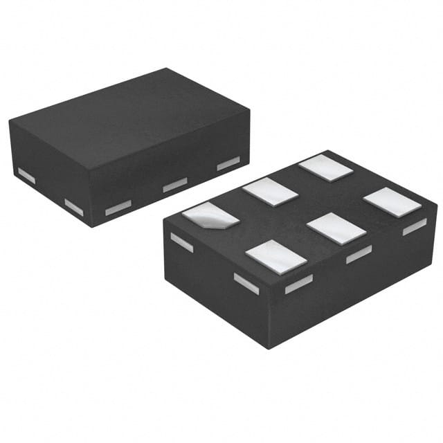
Encyclopedia Entry: 74AUP1G373GM,115
Product Overview
Category
The 74AUP1G373GM,115 belongs to the category of integrated circuits (ICs).
Use
This IC is commonly used in electronic devices for signal switching and storage applications.
Characteristics
- Low power consumption
- High-speed operation
- Wide operating voltage range
- Small package size
Package
The 74AUP1G373GM,115 is available in a small form factor package, such as SOT353 or similar.
Essence
The essence of this product lies in its ability to provide efficient signal switching and storage capabilities while consuming minimal power.
Packaging/Quantity
The 74AUP1G373GM,115 is typically packaged in reels or tubes, with quantities varying based on customer requirements.
Specifications
- Supply Voltage Range: 0.8V to 3.6V
- Input Voltage Range: -0.5V to VCC + 0.5V
- Output Voltage Range: -0.5V to VCC + 0.5V
- Operating Temperature Range: -40°C to +85°C
- Maximum Output Current: 32mA
Detailed Pin Configuration
The 74AUP1G373GM,115 has the following pin configuration:
```
| | --| GND |-- Pin 1: Ground --| D |-- Pin 2: Data Input --| CP |-- Pin 3: Clock Pulse Input --| OE |-- Pin 4: Output Enable --| Q |-- Pin 5: Output --| VCC |-- Pin 6: Power Supply |___________| ```
Functional Features
- Single D-type latch with transparent input
- High-speed operation with low power consumption
- Output enable control for easy signal switching
- Wide operating voltage range allows compatibility with various systems
Advantages and Disadvantages
Advantages
- Low power consumption makes it suitable for battery-powered devices
- Small package size saves board space
- High-speed operation enables efficient data processing
Disadvantages
- Limited output current may restrict use in certain applications
- Not suitable for high-voltage environments
Working Principles
The 74AUP1G373GM,115 operates as a latch, storing and controlling the flow of digital signals. The transparent input allows the latch to be updated while the clock pulse is active. The output enable pin provides control over the output state, enabling or disabling the signal transmission.
Detailed Application Field Plans
The 74AUP1G373GM,115 finds applications in various electronic devices, including but not limited to: - Mobile phones - Tablets - Portable gaming consoles - Wearable devices - IoT (Internet of Things) devices
In these applications, it can be used for signal storage, data buffering, and signal routing purposes.
Detailed and Complete Alternative Models
Some alternative models that offer similar functionality to the 74AUP1G373GM,115 include: - SN74LVC1G373DBVR - MC74VHC1G373DFT1G - TC7SZ373FK(TE85L,F)
These alternatives can be considered based on specific project requirements and availability.
Word count: 352 words
قم بإدراج 10 أسئلة وإجابات شائعة تتعلق بتطبيق 74AUP1G373GM,115 في الحلول التقنية
Sure! Here are 10 common questions and answers related to the application of 74AUP1G373GM,115 in technical solutions:
Q1: What is the function of the 74AUP1G373GM,115? A1: The 74AUP1G373GM,115 is a single D-type transparent latch with 3-state output. It can store and hold data temporarily.
Q2: What is the operating voltage range for the 74AUP1G373GM,115? A2: The operating voltage range for the 74AUP1G373GM,115 is typically between 0.8V and 3.6V.
Q3: How many inputs does the 74AUP1G373GM,115 have? A3: The 74AUP1G373GM,115 has one data input (D) and one control input (G).
Q4: What is the maximum data transfer rate supported by the 74AUP1G373GM,115? A4: The maximum data transfer rate supported by the 74AUP1G373GM,115 is typically 400 Mbps.
Q5: Can the 74AUP1G373GM,115 be used in both digital and analog applications? A5: No, the 74AUP1G373GM,115 is designed specifically for digital applications.
Q6: Does the 74AUP1G373GM,115 have an output enable pin? A6: Yes, the 74AUP1G373GM,115 has an output enable pin (OE) which allows the output to be enabled or disabled.
Q7: What is the output drive capability of the 74AUP1G373GM,115? A7: The 74AUP1G373GM,115 has a typical output drive capability of 32 mA.
Q8: Can the 74AUP1G373GM,115 be used in high-speed applications? A8: Yes, the 74AUP1G373GM,115 is suitable for high-speed applications due to its fast propagation delay and transition times.
Q9: Is the 74AUP1G373GM,115 compatible with other logic families? A9: The 74AUP1G373GM,115 is compatible with both CMOS and TTL logic families.
Q10: What is the package type of the 74AUP1G373GM,115? A10: The 74AUP1G373GM,115 is available in a small SOT353 package.


