

74AUP1G74GN,115
Basic Information Overview
- Category: Integrated Circuit (IC)
- Use: Flip-Flop
- Characteristics: Single D-type flip-flop with set and reset
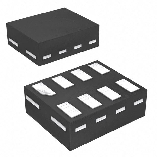
- Package: SOT353 (SC-88A)
- Essence: This IC is a single D-type flip-flop with set and reset functionality. It is designed for use in various digital applications.
- Packaging/Quantity: Available in reels of 3000 pieces
Specifications
- Supply Voltage Range: 0.8 V to 3.6 V
- High-Level Input Voltage: 0.7 x VDD to VDD + 0.3 V
- Low-Level Input Voltage: -0.3 V to 0.3 x VDD
- High-Level Output Voltage: 0.9 x VDD to VDD + 0.1 V
- Low-Level Output Voltage: 0 V to 0.1 x VDD
- Operating Temperature Range: -40°C to +125°C
Detailed Pin Configuration
The 74AUP1G74GN,115 IC has the following pin configuration:
```
| | --| CLR Q |-- VDD --| D GND |-- Q --| PR CLK |-- D |___________| ```
Functional Features
- Single D-type flip-flop with asynchronous set and reset inputs
- Positive-edge triggered clock input (CLK)
- Data input (D) for storing information
- Set input (PR) for forcing the output to a high level
- Reset input (CLR) for forcing the output to a low level
- Output (Q) provides the stored data
Advantages and Disadvantages
Advantages: - Compact size due to SOT353 package - Wide supply voltage range allows for versatile applications - Low power consumption - Easy integration into digital circuits
Disadvantages: - Limited number of flip-flops in a single package - Not suitable for high-speed applications
Working Principles
The 74AUP1G74GN,115 is a D-type flip-flop that stores data based on the positive-edge triggered clock input. The data input (D) determines the state of the output (Q). The set input (PR) forces the output to a high level, while the reset input (CLR) forces it to a low level.
Detailed Application Field Plans
The 74AUP1G74GN,115 IC can be used in various digital applications, including but not limited to: - Data storage and transfer systems - Clock synchronization circuits - State machine designs - Control systems - Communication devices
Detailed and Complete Alternative Models
Some alternative models that serve similar functions to the 74AUP1G74GN,115 IC include: - SN74LVC1G74DBVR - MC74VHC1GT74DF1G - TC7SZ74FU
These alternatives offer similar flip-flop functionality with slight variations in specifications and packaging options.
Word count: 275 words
قم بإدراج 10 أسئلة وإجابات شائعة تتعلق بتطبيق 74AUP1G74GN,115 في الحلول التقنية
Sure! Here are 10 common questions and answers related to the application of 74AUP1G74GN,115 in technical solutions:
Q1: What is the 74AUP1G74GN,115? A1: The 74AUP1G74GN,115 is a single D-type flip-flop with set and reset inputs. It is a digital logic component used for storing and manipulating binary data.
Q2: What is the operating voltage range of the 74AUP1G74GN,115? A2: The operating voltage range of the 74AUP1G74GN,115 is from 0.8V to 3.6V.
Q3: What is the maximum clock frequency supported by the 74AUP1G74GN,115? A3: The maximum clock frequency supported by the 74AUP1G74GN,115 is typically around 500 MHz.
Q4: Can the 74AUP1G74GN,115 be used in battery-powered applications? A4: Yes, the 74AUP1G74GN,115 can be used in battery-powered applications as it operates within a low voltage range.
Q5: How many flip-flops are there in the 74AUP1G74GN,115? A5: The 74AUP1G74GN,115 consists of a single flip-flop.
Q6: What is the power consumption of the 74AUP1G74GN,115? A6: The power consumption of the 74AUP1G74GN,115 is relatively low due to its low voltage operation.
Q7: Can the 74AUP1G74GN,115 be cascaded to create larger memory storage? A7: Yes, multiple 74AUP1G74GN,115 flip-flops can be cascaded to create larger memory storage or more complex digital circuits.
Q8: What is the typical propagation delay of the 74AUP1G74GN,115? A8: The typical propagation delay of the 74AUP1G74GN,115 is around 2.5 ns.
Q9: Can the 74AUP1G74GN,115 be used in high-speed data transmission applications? A9: Yes, the 74AUP1G74GN,115 can be used in high-speed data transmission applications due to its relatively fast operation.
Q10: Is the 74AUP1G74GN,115 compatible with other logic families? A10: Yes, the 74AUP1G74GN,115 is compatible with a wide range of logic families, making it versatile for integration into various technical solutions.
Please note that these answers are general and may vary depending on specific datasheet specifications and application requirements.