

Encyclopedia Entry: 74AUP1G97UKZ
Product Overview
Category
The 74AUP1G97UKZ belongs to the category of integrated circuits (ICs).
Use
This IC is commonly used in electronic devices for signal switching and amplification purposes.
Characteristics
- Low power consumption
- High-speed operation
- Small package size
- Wide operating voltage range
Package
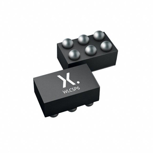
The 74AUP1G97UKZ is available in a small form factor package, such as SOT353 or XSON6.
Essence
The essence of this product lies in its ability to provide efficient signal switching and amplification functions while consuming minimal power.
Packaging/Quantity
The 74AUP1G97UKZ is typically packaged in reels or tubes, with quantities varying depending on the manufacturer's specifications.
Specifications
- Supply Voltage Range: 0.8V to 3.6V
- Input Voltage Range: 0V to VCC
- Output Voltage Range: 0V to VCC
- Operating Temperature Range: -40°C to +85°C
- Maximum Output Current: 32mA
Detailed Pin Configuration
The 74AUP1G97UKZ has the following pin configuration:
____
   NC |    | VCC
 IN1  |    | OUT
 GND  |____| IN2
Functional Features
- Single-channel signal switching
- High-speed operation
- Low power consumption
- Wide operating voltage range
- Schmitt-trigger input for noise immunity
Advantages and Disadvantages
Advantages
- Low power consumption makes it suitable for battery-powered devices.
- High-speed operation enables quick signal processing.
- Small package size allows for space-efficient designs.
- Wide operating voltage range provides flexibility in various applications.
Disadvantages
- Limited output current may restrict its use in high-power applications.
- Lack of multiple channels limits its capability for complex signal routing.
Working Principles
The 74AUP1G97UKZ operates based on CMOS (Complementary Metal-Oxide-Semiconductor) technology. It utilizes a combination of MOSFETs (Metal-Oxide-Semiconductor Field-Effect Transistors) to achieve signal switching and amplification. The Schmitt-trigger input ensures reliable operation by providing noise immunity.
Detailed Application Field Plans
The 74AUP1G97UKZ finds application in various electronic devices, including but not limited to: - Mobile phones - Tablets - Portable media players - Wearable devices - IoT (Internet of Things) devices
In these applications, it can be used for signal routing, level shifting, or amplification tasks.
Detailed Alternative Models
Some alternative models that offer similar functionality to the 74AUP1G97UKZ include: - SN74LVC1G97DBVR - MC74VHC1G97DFT1G - TC7SZU04FU
These alternatives can be considered based on specific requirements such as voltage range, package size, or additional features.
Word count: 346 words
قم بإدراج 10 أسئلة وإجابات شائعة تتعلق بتطبيق 74AUP1G97UKZ في الحلول التقنية
Question: What is the purpose of the 74AUP1G97UKZ in technical solutions?
Answer: The 74AUP1G97UKZ is a single buffer/driver IC that can be used to amplify and buffer digital signals in various technical solutions.Question: What is the operating voltage range of the 74AUP1G97UKZ?
Answer: The 74AUP1G97UKZ operates within a voltage range of 0.8V to 3.6V, making it suitable for low-power applications.Question: Can the 74AUP1G97UKZ handle high-speed signals?
Answer: Yes, the 74AUP1G97UKZ has a maximum propagation delay of 2.5ns, which allows it to handle high-speed signals effectively.Question: How many inputs and outputs does the 74AUP1G97UKZ have?
Answer: The 74AUP1G97UKZ has one input and one output, making it a single buffer/driver.Question: Is the 74AUP1G97UKZ compatible with different logic families?
Answer: Yes, the 74AUP1G97UKZ is compatible with various logic families, including CMOS, TTL, and LVCMOS.Question: Can the 74AUP1G97UKZ be used in battery-powered devices?
Answer: Absolutely, the 74AUP1G97UKZ is designed for low-power applications and can operate efficiently in battery-powered devices.Question: What is the maximum current that the 74AUP1G97UKZ can source or sink?
Answer: The 74AUP1G97UKZ can source or sink up to 32mA of current, making it suitable for driving moderate loads.Question: Does the 74AUP1G97UKZ have any built-in protection features?
Answer: Yes, the 74AUP1G97UKZ has built-in ESD protection, which helps safeguard the IC from electrostatic discharge events.Question: Can the 74AUP1G97UKZ be used in automotive applications?
Answer: Yes, the 74AUP1G97UKZ is AEC-Q100 qualified, making it suitable for use in automotive electronics.Question: What is the package type of the 74AUP1G97UKZ?
Answer: The 74AUP1G97UKZ is available in a small SOT353 package, which is compact and space-saving.