

Encyclopedia Entry: 74AUP2G241GF,115
Product Overview
Category
The 74AUP2G241GF,115 belongs to the category of integrated circuits (ICs).
Use
This IC is commonly used in electronic devices for signal amplification and switching purposes.
Characteristics
- Low power consumption
- High-speed operation
- Wide operating voltage range
- Small package size
Package
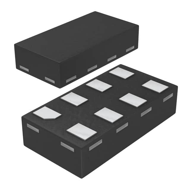
The 74AUP2G241GF,115 is available in a small form factor package, such as SOT353 or XSON6.
Essence
This IC is designed to provide efficient signal amplification and switching capabilities while consuming minimal power.
Packaging/Quantity
The 74AUP2G241GF,115 is typically packaged in reels or tubes, with quantities varying based on customer requirements.
Specifications
- Supply Voltage Range: 1.65V to 5.5V
- Input Voltage Range: -0.5V to VCC + 0.5V
- Output Voltage Range: GND to VCC
- Operating Temperature Range: -40°C to +85°C
- Maximum Output Current: ±24mA
Detailed Pin Configuration
The 74AUP2G241GF,115 has a total of six pins arranged as follows:
___________
   OE | 1       6 | VCC
 I/O1 | 2       5 | I/O2
  GND | 3       4 | A1
       ‾‾‾‾‾‾‾‾‾‾‾
Functional Features
- Dual buffer gates with independent control
- Non-inverting outputs
- Enable/disable function for each gate
- High-speed operation suitable for various applications
Advantages and Disadvantages
Advantages
- Low power consumption makes it suitable for battery-powered devices
- Wide operating voltage range allows compatibility with different systems
- Small package size saves board space in compact designs
Disadvantages
- Limited output current may not be suitable for high-power applications
- Lack of built-in protection features against overvoltage or ESD events
Working Principles
The 74AUP2G241GF,115 operates as a dual buffer gate. It amplifies and switches input signals based on the control inputs and provides non-inverted outputs. The enable/disable function allows independent control of each gate, providing flexibility in signal routing.
Detailed Application Field Plans
The 74AUP2G241GF,115 finds applications in various electronic devices, including but not limited to: - Mobile phones - Tablets - Portable media players - Wearable devices - IoT devices
It is commonly used in signal amplification, level shifting, and signal buffering circuits within these devices.
Detailed and Complete Alternative Models
Some alternative models that offer similar functionality to the 74AUP2G241GF,115 include: - SN74LVC2G241 - NC7WZ241 - TC7SZ241FU
These alternatives can be considered based on specific design requirements and availability.
Word count: 314 words
قم بإدراج 10 أسئلة وإجابات شائعة تتعلق بتطبيق 74AUP2G241GF,115 في الحلول التقنية
Sure! Here are 10 common questions and answers related to the application of 74AUP2G241GF,115 in technical solutions:
Q: What is the function of the 74AUP2G241GF,115? A: The 74AUP2G241GF,115 is a dual buffer/line driver IC that can be used for signal amplification and buffering.
Q: What is the operating voltage range of the 74AUP2G241GF,115? A: The operating voltage range of this IC is typically between 0.8V and 3.6V.
Q: Can the 74AUP2G241GF,115 handle high-speed signals? A: Yes, this IC is designed to handle high-speed signals with a maximum propagation delay of 2.5 ns.
Q: Is the 74AUP2G241GF,115 compatible with both CMOS and TTL logic levels? A: Yes, this IC is compatible with both CMOS and TTL logic levels, making it versatile for various applications.
Q: What is the output drive strength of the 74AUP2G241GF,115? A: The output drive strength of this IC is typically 24 mA, allowing it to drive capacitive loads efficiently.
Q: Can the 74AUP2G241GF,115 be used in battery-powered applications? A: Yes, this IC has a low power consumption and can be used in battery-powered applications.
Q: Does the 74AUP2G241GF,115 have built-in ESD protection? A: Yes, this IC has built-in ESD protection, ensuring robustness against electrostatic discharge events.
Q: What is the package type of the 74AUP2G241GF,115? A: The 74AUP2G241GF,115 is available in a small SOT353 package, which is suitable for space-constrained designs.
Q: Can the 74AUP2G241GF,115 be used in automotive applications? A: Yes, this IC is AEC-Q100 qualified and can be used in automotive applications that require high reliability.
Q: Are there any application notes or reference designs available for the 74AUP2G241GF,115? A: Yes, the manufacturer provides application notes and reference designs to help users implement the IC effectively in their designs.
Please note that the answers provided here are general and may vary depending on specific datasheet specifications and application requirements.