

Encyclopedia Entry: 74AUP2G80GF,115
Product Overview
Category
The 74AUP2G80GF,115 belongs to the category of integrated circuits (ICs).
Use
This IC is commonly used in electronic devices for various applications, including signal processing, amplification, and logic operations.
Characteristics
- Low power consumption
- High-speed operation
- Small form factor
- Wide operating voltage range
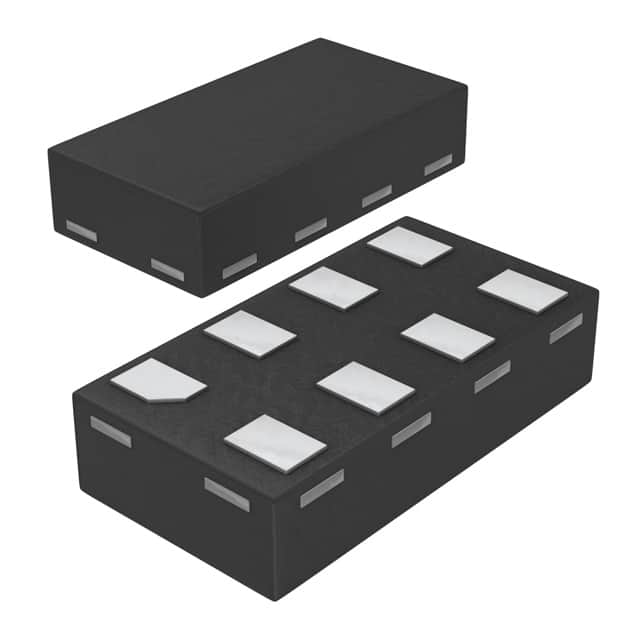
Package
The 74AUP2G80GF,115 is available in a compact package, typically a small-outline transistor (SOT) or a flip-chip package.
Essence
This IC is designed to provide efficient and reliable performance in digital circuitry by integrating multiple functions into a single chip.
Packaging/Quantity
The 74AUP2G80GF,115 is usually packaged in reels or tubes, with quantities varying depending on the manufacturer's specifications.
Specifications
- Supply Voltage: 1.65V to 5.5V
- Operating Temperature Range: -40°C to +85°C
- Input/Output Logic Levels: CMOS/TTL compatible
- Maximum Output Current: 32mA
- Propagation Delay: <10ns
Detailed Pin Configuration
The 74AUP2G80GF,115 has a total of 6 pins arranged as follows:
```
| | --| 1 2 |-- --| 3 4 |-- --| 5 6 |-- |___________| ```
Pin Configuration: 1. Input A 2. Input B 3. Ground (GND) 4. Output Y 5. Power Supply (VCC) 6. Enable (EN)
Functional Features
- Dual-input AND gate functionality
- High-speed operation for efficient signal processing
- Low power consumption for energy-efficient designs
- Wide operating voltage range allows compatibility with various systems
- Schmitt-trigger input for noise immunity
Advantages and Disadvantages
Advantages
- Compact size enables integration into space-constrained devices
- Low power consumption prolongs battery life in portable applications
- High-speed operation facilitates rapid data processing
- Wide operating voltage range enhances versatility in different environments
Disadvantages
- Limited number of inputs and outputs restricts complex circuit designs
- Sensitivity to electrostatic discharge (ESD) requires proper handling during assembly and usage
Working Principles
The 74AUP2G80GF,115 operates based on the principles of digital logic gates. It performs the logical AND operation on the input signals A and B, producing an output signal Y. The enable pin (EN) controls the functionality of the gate, allowing or inhibiting the output.
Detailed Application Field Plans
The 74AUP2G80GF,115 finds extensive use in various electronic applications, including but not limited to: - Microcontrollers and microprocessors - Communication systems - Consumer electronics - Automotive electronics - Industrial automation
Detailed and Complete Alternative Models
- 74AUP1G80GF,115: Single-input AND gate IC
- 74AUP2G08GF,115: Dual-input OR gate IC
- 74AUP3G14GF,115: Triple-input Schmitt-trigger inverter IC
- 74AUP4G125GF,115: Quad-buffer gate IC
These alternative models offer similar functionality and characteristics, providing flexibility in circuit design choices.
In conclusion, the 74AUP2G80GF,115 is a versatile integrated circuit that combines dual-input AND gate functionality with low power consumption and high-speed operation. Its compact size and wide operating voltage range make it suitable for various electronic applications. However, designers should consider its limitations in terms of input/output count and sensitivity to ESD.
قم بإدراج 10 أسئلة وإجابات شائعة تتعلق بتطبيق 74AUP2G80GF,115 في الحلول التقنية
Sure! Here are 10 common questions and answers related to the application of 74AUP2G80GF,115 in technical solutions:
Q: What is the function of the 74AUP2G80GF,115? A: The 74AUP2G80GF,115 is a dual D-type flip-flop with set and reset inputs.
Q: What is the operating voltage range for the 74AUP2G80GF,115? A: The operating voltage range is from 0.8V to 3.6V.
Q: Can the 74AUP2G80GF,115 be used in battery-powered applications? A: Yes, the low operating voltage range makes it suitable for battery-powered applications.
Q: What is the maximum clock frequency supported by the 74AUP2G80GF,115? A: The maximum clock frequency is typically around 200MHz.
Q: Does the 74AUP2G80GF,115 have any built-in protection features? A: Yes, it has built-in ESD protection on all inputs and outputs.
Q: Can I use the 74AUP2G80GF,115 in high-speed data transmission applications? A: Yes, it can be used in high-speed data transmission applications due to its fast propagation delay.
Q: How many inputs and outputs does the 74AUP2G80GF,115 have? A: It has two inputs (D and CLK) and two outputs (Q and Q̅).
Q: Is the 74AUP2G80GF,115 compatible with other logic families? A: Yes, it is compatible with both CMOS and TTL logic families.
Q: Can I cascade multiple 74AUP2G80GF,115 flip-flops together? A: Yes, you can cascade multiple flip-flops to create larger counters or shift registers.
Q: What is the package type for the 74AUP2G80GF,115? A: It is available in a small SOT353 package.
Please note that these answers are general and may vary depending on the specific application and requirements.