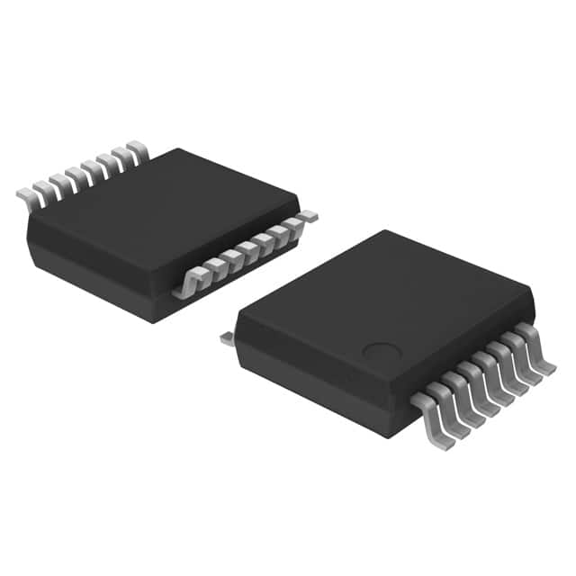
74HC137DB,112
Product Overview
- Category: Integrated Circuit (IC)
- Use: Decoding and Demultiplexing
- Characteristics: High-speed operation, low power consumption
- Package: SOIC (Small Outline Integrated Circuit)
- Essence: A 3-to-8 line decoder/demultiplexer with active-low outputs
- Packaging/Quantity: Tape and Reel, 2500 units per reel
Specifications
- Supply Voltage Range: 2.0V to 6.0V
- Input Voltage Range: -0.5V to VCC + 0.5V
- Output Voltage Range: -0.5V to VCC + 0.5V
- Operating Temperature Range: -40°C to +125°C
- Propagation Delay Time: 15 ns (typical)
Detailed Pin Configuration
The 74HC137DB,112 has a total of 16 pins. The pin configuration is as follows:
- GND (Ground)
- A0 (Address Input 0)
- A1 (Address Input 1)
- A2 (Address Input 2)
- E1 (Enable Input 1)
- Y0 (Output 0)
- Y1 (Output 1)
- Y2 (Output 2)
- Y3 (Output 3)
- Y4 (Output 4)
- Y5 (Output 5)
- Y6 (Output 6)
- Y7 (Output 7)
- E2 (Enable Input 2)
- VCC (Positive Power Supply)
- NC (No Connection)
Functional Features
The 74HC137DB,112 is designed to decode three binary address inputs (A0, A1, A2) into eight mutually exclusive active-low outputs (Y0-Y7). It features two enable inputs (E1, E2) that can be used to disable the outputs independently. The IC operates at high speed and consumes low power, making it suitable for various decoding and demultiplexing applications.
Advantages and Disadvantages
Advantages: - High-speed operation - Low power consumption - Compact SOIC package - Wide supply voltage range
Disadvantages: - Limited number of address inputs (3) - Active-low outputs may require additional circuitry for certain applications
Working Principles
The 74HC137DB,112 works by interpreting the binary values applied to the address inputs (A0-A2) and generating a corresponding active-low output signal on one of the eight output pins (Y0-Y7). The enable inputs (E1, E2) control the activation of the outputs. When an enable input is low, the corresponding outputs are disabled.
Detailed Application Field Plans
The 74HC137DB,112 can be used in various applications, including but not limited to: - Address decoding in microcontrollers and microprocessors - Data demultiplexing in communication systems - Memory selection in digital systems - Control signal generation in industrial automation
Detailed and Complete Alternative Models
Some alternative models that offer similar functionality to the 74HC137DB,112 include: - 74LS138: A TTL (Transistor-Transistor Logic) version of the decoder/demultiplexer - CD74HC238: A higher voltage version with additional address inputs - SN74HCT138: A CMOS (Complementary Metal-Oxide-Semiconductor) version with improved noise immunity
These alternatives can be considered based on specific requirements and compatibility with existing designs.
Word count: 346 words
قم بإدراج 10 أسئلة وإجابات شائعة تتعلق بتطبيق 74HC137DB,112 في الحلول التقنية
Sure! Here are 10 common questions and answers related to the application of 74HC137DB,112 in technical solutions:
Q: What is the function of the 74HC137DB,112? A: The 74HC137DB,112 is a 3-to-8 line decoder/demultiplexer IC that converts binary input signals into output lines.
Q: What is the maximum operating voltage for the 74HC137DB,112? A: The maximum operating voltage for the 74HC137DB,112 is typically 5.5V.
Q: How many input lines does the 74HC137DB,112 have? A: The 74HC137DB,112 has three input lines (A0, A1, and A2) which are used to select one of the eight output lines.
Q: What is the purpose of the enable (E) pin on the 74HC137DB,112? A: The enable (E) pin is used to enable or disable the operation of the decoder/demultiplexer. When E is high, the outputs are active.
Q: Can the 74HC137DB,112 be cascaded to increase the number of output lines? A: Yes, multiple 74HC137DB,112 ICs can be cascaded together to increase the number of output lines.
Q: What is the typical propagation delay of the 74HC137DB,112? A: The typical propagation delay of the 74HC137DB,112 is around 15 ns.
Q: Can the 74HC137DB,112 be used with both TTL and CMOS logic levels? A: Yes, the 74HC137DB,112 is compatible with both TTL and CMOS logic levels.
Q: What is the maximum output current of the 74HC137DB,112? A: The maximum output current per output pin of the 74HC137DB,112 is typically 4 mA.
Q: Can the 74HC137DB,112 be used in high-speed applications? A: Yes, the 74HC137DB,112 is designed for high-speed operation and can be used in various high-speed applications.
Q: Are there any specific precautions to consider when using the 74HC137DB,112? A: It is important to ensure that the power supply voltage does not exceed the specified maximum voltage, and to avoid static discharge during handling to prevent damage to the IC.
Please note that these answers are general and may vary depending on the specific datasheet and manufacturer's specifications for the 74HC137DB,112.


