

74HC2G66GD,125
Basic Information Overview
- Category: Integrated Circuit (IC)
- Use: Digital Logic Switch
- Characteristics: High-speed operation, low power consumption
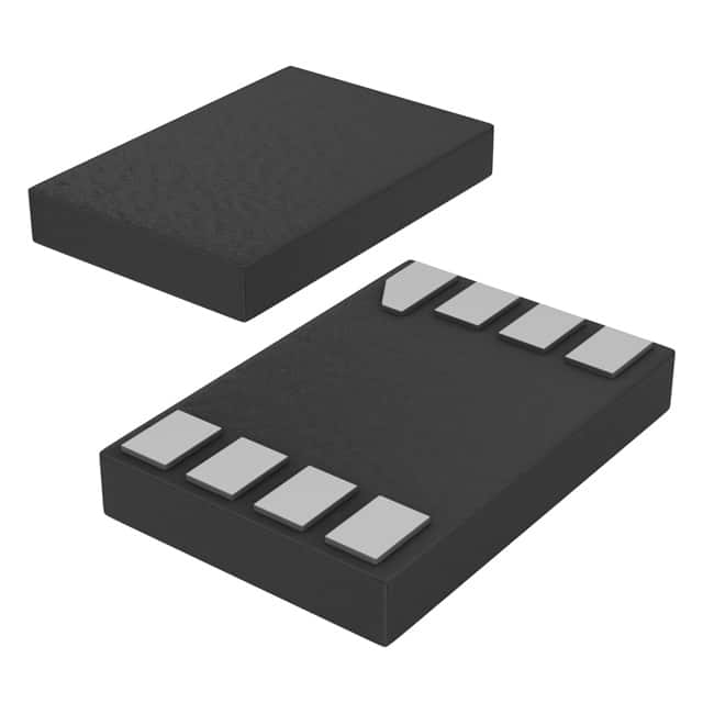
- Package: SOT353 (Thin Shrink Small Outline Package)
- Essence: Dual bilateral switch
- Packaging/Quantity: Tape and Reel, 3000 pieces per reel
Specifications
- Supply Voltage Range: 2.0V to 6.0V
- High-Level Input Voltage: 0.7 x VCC
- Low-Level Input Voltage: 0.3 x VCC
- High-Level Output Current: -32 mA
- Low-Level Output Current: 32 mA
- Operating Temperature Range: -40°C to +125°C
Detailed Pin Configuration
The 74HC2G66GD,125 has a total of 8 pins arranged as follows:
____
   A1 |o    | VCC
   B1 |     | Y1
   A2 |     | Y2
   B2 |_____| GND
Functional Features
- Dual bilateral switch with independent control inputs
- Wide supply voltage range allows compatibility with various systems
- High-speed operation enables efficient signal switching
- Low power consumption for energy-efficient applications
- Break-before-make switching action ensures no short circuits during transition
Advantages
- Compact package size saves board space
- Wide operating temperature range allows usage in extreme environments
- High-level output current capability facilitates driving of external loads
- Low-level output current capability supports bidirectional signal transmission
Disadvantages
- Limited number of channels (2) may restrict certain applications requiring more switches
- Sensitive to electrostatic discharge (ESD), necessitating proper handling precautions
Working Principles
The 74HC2G66GD,125 is a dual bilateral switch that allows the transfer of digital signals between two independent channels. It operates based on the principle of field-effect transistors (FETs) acting as electronic switches. The control inputs (A1, B1, A2, B2) determine the state of the switches, either open or closed, allowing or blocking signal flow.
Detailed Application Field Plans
The 74HC2G66GD,125 finds applications in various fields, including: 1. Communication Systems: Signal routing and switching in telecommunication equipment. 2. Test and Measurement Instruments: Multiplexing and signal routing in test equipment. 3. Consumer Electronics: Audio and video signal switching in TVs, set-top boxes, and gaming consoles. 4. Industrial Automation: Control signal routing in PLCs (Programmable Logic Controllers). 5. Automotive Electronics: Signal switching in automotive infotainment systems.
Detailed and Complete Alternative Models
- SN74LVC2G66: Similar dual bilateral switch with lower power consumption.
- CD4066B: Quad bilateral switch with higher channel count.
- TS5A3160: Single-pole double-throw (SPDT) analog switch with similar characteristics.
Note: This is not an exhaustive list, and there are several other alternative models available in the market.
In conclusion, the 74HC2G66GD,125 is a versatile integrated circuit that serves as a dual bilateral switch. Its high-speed operation, low power consumption, and compact package make it suitable for various applications in communication systems, consumer electronics, industrial automation, and automotive electronics. While it has limitations in terms of channel count, proper handling and consideration of alternative models can overcome these drawbacks.
قم بإدراج 10 أسئلة وإجابات شائعة تتعلق بتطبيق 74HC2G66GD,125 في الحلول التقنية
Sure! Here are 10 common questions and answers related to the application of 74HC2G66GD,125 in technical solutions:
Q: What is the 74HC2G66GD,125?
A: The 74HC2G66GD,125 is a dual bilateral analog switch IC that can be used for various applications in electronic circuits.Q: What is the maximum voltage rating of the 74HC2G66GD,125?
A: The maximum voltage rating of the 74HC2G66GD,125 is typically around 5.5V.Q: Can the 74HC2G66GD,125 handle both analog and digital signals?
A: Yes, the 74HC2G66GD,125 can handle both analog and digital signals, making it versatile for different applications.Q: What is the typical on-resistance of the 74HC2G66GD,125?
A: The typical on-resistance of the 74HC2G66GD,125 is around 50 ohms.Q: How many channels does the 74HC2G66GD,125 have?
A: The 74HC2G66GD,125 has two independent channels, allowing for simultaneous switching of multiple signals.Q: Can the 74HC2G66GD,125 be used in low-power applications?
A: Yes, the 74HC2G66GD,125 is designed for low-power consumption, making it suitable for battery-powered devices.Q: What is the operating temperature range of the 74HC2G66GD,125?
A: The operating temperature range of the 74HC2G66GD,125 is typically between -40°C to 85°C.Q: Can the 74HC2G66GD,125 be used for audio signal switching?
A: Yes, the 74HC2G66GD,125 can be used for audio signal switching as it has low distortion and high bandwidth capabilities.Q: Is the 74HC2G66GD,125 compatible with both CMOS and TTL logic levels?
A: Yes, the 74HC2G66GD,125 is compatible with both CMOS and TTL logic levels, providing flexibility in different circuit designs.Q: What package options are available for the 74HC2G66GD,125?
A: The 74HC2G66GD,125 is available in various package options, such as SOT353 and XSON6, allowing for different mounting preferences.
Please note that the answers provided here are general and may vary depending on specific datasheet specifications and application requirements.