

Encyclopedia Entry: 74HCT259BQ,115
Product Overview
- Category: Integrated Circuit (IC)
- Use: Digital Logic Device
- Characteristics: High-Speed, CMOS Technology
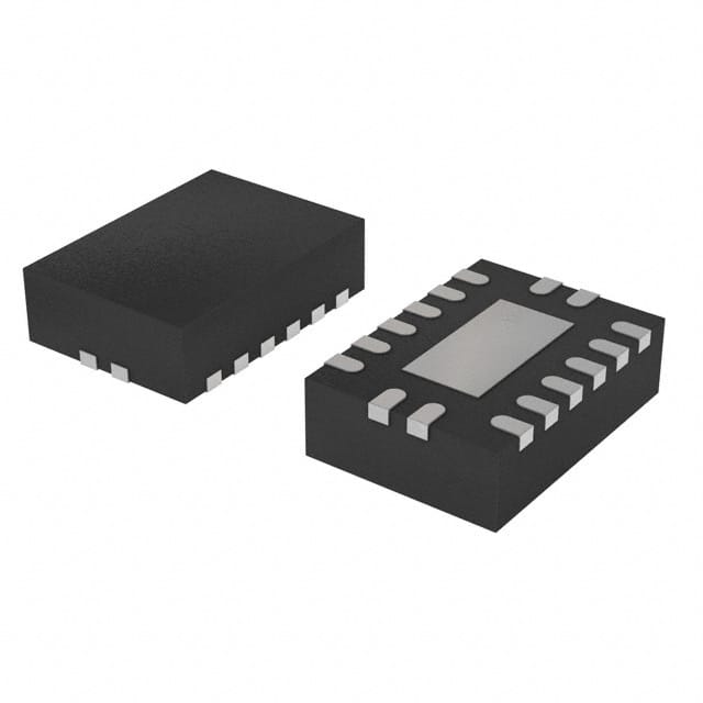
- Package: SOIC (Small Outline Integrated Circuit)
- Essence: 8-Bit Addressable Latch/Shift Register
- Packaging/Quantity: Tape and Reel, 2500 units per reel
Specifications
- Supply Voltage Range: 2.0V to 6.0V
- Input Voltage Range: 0V to VCC
- Output Voltage Range: 0V to VCC
- Operating Temperature Range: -40°C to +125°C
- Maximum Clock Frequency: 80 MHz
- Number of Inputs/Outputs: 16
- Logic Family: HCT (High-Speed CMOS)
Detailed Pin Configuration
- GND (Ground)
- SER (Serial Data Input)
- QA (Output A)
- QB (Output B)
- QC (Output C)
- QD (Output D)
- QE (Output E)
- QF (Output F)
- QG (Output G)
- QH (Output H)
- MR (Master Reset)
- SH/LD (Shift/Load)
- CLK (Clock Input)
- OE (Output Enable)
- VCC (Supply Voltage)
- NC (No Connection)
Functional Features
- 8-bit addressable latch with serial input and parallel output capability
- Can be used as a shift register or storage register
- Serial data is shifted into the device on each rising edge of the clock signal
- Parallel outputs are updated when the shift/load input is low
- Master reset input allows clearing all outputs to a low state
- Output enable input allows disabling the outputs
Advantages
- High-speed operation due to CMOS technology
- Wide supply voltage range allows compatibility with various systems
- Versatile functionality as both a latch and shift register
- Compact SOIC package for space-saving designs
- Easy integration into existing digital logic circuits
Disadvantages
- Limited number of inputs/outputs (16)
- Requires external clock signal for operation
- Not suitable for high-voltage applications
Working Principles
The 74HCT259BQ,115 is an 8-bit addressable latch/shift register that can be used in various digital logic applications. It operates based on CMOS technology, which provides high-speed performance and low power consumption. The device has a serial data input (SER) and parallel outputs (QA-QH). When the shift/load input (SH/LD) is low, the serial data is shifted into the device on each rising edge of the clock input (CLK). The parallel outputs are updated when the shift/load input is low, allowing the stored data to be latched and outputted. The master reset input (MR) clears all outputs to a low state, while the output enable input (OE) can disable the outputs.
Detailed Application Field Plans
The 74HCT259BQ,115 can be utilized in various digital systems and applications, including: 1. Address decoding in microcontrollers and microprocessors 2. Data storage and retrieval in memory systems 3. Serial-to-parallel or parallel-to-serial data conversion 4. Multiplexing and demultiplexing of data signals 5. Control and sequencing of digital circuits 6. Shift register-based counters and timers 7. Interface circuitry between different logic families
Detailed and Complete Alternative Models
- 74HC595: 8-Bit Serial-In, Parallel-Out Shift Register
- CD4015: Dual 4-Stage Static Shift Register
- SN74LS164: 8-Bit Serial-In, Parallel-Out Shift Register
- CD4094: 8-Stage Shift-and-Store Bus Register
- MC74HC595A: 8-Bit Serial-In, Parallel-Out Shift Register
Note: The above list is not exhaustive and there are several other alternative models available in the market.
In conclusion, the 74HCT259BQ,115 is a versatile integrated circuit that combines the functionality of an 8-bit addressable latch and shift register. Its high-speed operation, wide supply voltage range, and compact package make it suitable for various digital logic applications. However, it has limitations in terms of the number of inputs/outputs and voltage compatibility. Engineers can consider alternative models based on their specific requirements and system constraints.
قم بإدراج 10 أسئلة وإجابات شائعة تتعلق بتطبيق 74HCT259BQ,115 في الحلول التقنية
Sure! Here are 10 common questions and answers related to the application of 74HCT259BQ,115 in technical solutions:
Question: What is the function of the 74HCT259BQ,115?
Answer: The 74HCT259BQ,115 is an 8-bit addressable latch with three-state outputs. It can store and output data based on the control signals.Question: What is the operating voltage range for the 74HCT259BQ,115?
Answer: The operating voltage range for this IC is typically between 4.5V and 5.5V.Question: How many inputs and outputs does the 74HCT259BQ,115 have?
Answer: This IC has 8 inputs (A0-A7), 8 outputs (O0-O7), and additional control inputs (G, LE, and OE).Question: Can the 74HCT259BQ,115 be used as a bidirectional buffer?
Answer: No, it is not designed for bidirectional operation. It is primarily used as an addressable latch.Question: What is the maximum clock frequency supported by the 74HCT259BQ,115?
Answer: The maximum clock frequency for reliable operation is typically around 25 MHz.Question: How can I cascade multiple 74HCT259BQ,115 ICs together?
Answer: You can connect the outputs of one IC to the inputs of the next IC in a daisy-chain configuration to achieve cascading.Question: What is the purpose of the G (Gate) input in the 74HCT259BQ,115?
Answer: The G input is used to enable or disable the latch. When G is low, the latch is enabled and data can be stored or outputted.Question: How does the LE (Latch Enable) input work in the 74HCT259BQ,115?
Answer: The LE input is used to control the latching of data. When LE transitions from high to low, the data on the inputs is latched and stored.Question: What is the function of the OE (Output Enable) input in the 74HCT259BQ,115?
Answer: The OE input is used to enable or disable the outputs. When OE is low, the outputs are enabled and can drive external circuitry.Question: Can the 74HCT259BQ,115 be used in both synchronous and asynchronous applications?
Answer: Yes, it can be used in both synchronous and asynchronous applications depending on how the control signals are utilized.
Please note that these answers are general and may vary based on specific application requirements.