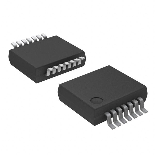
74LVC125ADB,118
Basic Information Overview
- Category: Integrated Circuit (IC)
- Use: Buffer/Driver
- Characteristics: Low Voltage CMOS Quad Buffer with 3-State Outputs
- Package: SOIC-14
- Essence: Logic Level Shifter and Signal Buffer
- Packaging/Quantity: Tape and Reel, 2500 pieces per reel
Specifications
- Supply Voltage Range: 1.65V to 5.5V
- High-Level Input Voltage: 2V to VCC + 0.5V
- Low-Level Input Voltage: -0.5V to 0.8V
- High-Level Output Voltage: 2.4V (min) at IOH = -4mA
- Low-Level Output Voltage: 0.4V (max) at IOL = 4mA
- Maximum Operating Frequency: 400MHz
- Propagation Delay: 4.3ns (typical)
Detailed Pin Configuration
The 74LVC125ADB,118 IC has a total of 14 pins arranged as follows:
___________
   1 |             | 14
   2 |             | 13
   3 |             | 12
   4 |             | 11
   5 |             | 10
   6 |             | 9
   7 |_____________| 8
Pin Description: 1. GND: Ground 2. A1: Input 1 3. Y1: Output 1 4. A2: Input 2 5. Y2: Output 2 6. OE: Output Enable 7. VCC: Power Supply
Functional Features
- Quad buffer with 3-state outputs
- Compatible with both 3.3V and 5V systems
- Provides voltage level shifting between different logic levels
- Allows bidirectional data flow
- High-speed operation with low power consumption
- Supports hot insertion
Advantages and Disadvantages
Advantages: - Wide supply voltage range allows compatibility with various systems - Low propagation delay enables high-speed operation - 3-state outputs provide flexibility in controlling bus lines - Small package size saves board space
Disadvantages: - Limited output current capability - Not suitable for high-power applications
Working Principles
The 74LVC125ADB,118 is a buffer IC that acts as an interface between different logic levels. It takes input signals from one logic level and provides buffered output signals at another logic level. The IC uses CMOS technology, allowing it to operate at low voltages while providing high-speed performance.
The buffer has four independent channels, each with an input and an output. The output enable (OE) pin controls the state of the outputs. When OE is high, the outputs are in a high-impedance state, allowing other devices to drive the bus lines. When OE is low, the inputs are transferred to the outputs with minimal delay.
Detailed Application Field Plans
The 74LVC125ADB,118 is commonly used in various digital systems where voltage level shifting and signal buffering are required. Some typical application fields include: - Microcontrollers and microprocessors - Communication systems - Data acquisition systems - Industrial automation - Consumer electronics
Detailed and Complete Alternative Models
- SN74LVC125A: Similar quad buffer IC from Texas Instruments
- MC74LCX125: Quad buffer IC with 5V tolerant inputs from ON Semiconductor
- CD74HCT125: Quad buffer IC with TTL-compatible inputs from Texas Instruments
- 74HC125: Quad buffer IC with higher output current capability from NXP Semiconductors
These alternative models offer similar functionality and can be used as replacements for the 74LVC125ADB,118 in various applications.
Word count: 460 words
قم بإدراج 10 أسئلة وإجابات شائعة تتعلق بتطبيق 74LVC125ADB,118 في الحلول التقنية
Sure! Here are 10 common questions and answers related to the application of 74LVC125ADB,118 in technical solutions:
1. What is the function of the 74LVC125ADB,118? The 74LVC125ADB,118 is a quad buffer/line driver with 3-state outputs. It is used to control the flow of data between different parts of a circuit.
2. What is the voltage supply range for the 74LVC125ADB,118? The voltage supply range for the 74LVC125ADB,118 is typically between 1.65V and 5.5V.
3. How many buffers/line drivers are there in the 74LVC125ADB,118? The 74LVC125ADB,118 has four buffers/line drivers, each with a separate input and output.
4. What is the maximum output current of the 74LVC125ADB,118? The maximum output current of the 74LVC125ADB,118 is typically 24mA.
5. Can the 74LVC125ADB,118 be used for bidirectional communication? No, the 74LVC125ADB,118 is not designed for bidirectional communication. It is meant for unidirectional data transfer.
6. What is the propagation delay of the 74LVC125ADB,118? The propagation delay of the 74LVC125ADB,118 is typically around 4.3ns.
7. Is the 74LVC125ADB,118 compatible with TTL logic levels? Yes, the 74LVC125ADB,118 is compatible with both TTL and CMOS logic levels.
8. Can the 74LVC125ADB,118 drive capacitive loads? Yes, the 74LVC125ADB,118 can drive capacitive loads up to a certain limit. It is recommended to refer to the datasheet for specific details.
9. What is the power dissipation of the 74LVC125ADB,118? The power dissipation of the 74LVC125ADB,118 depends on the operating conditions and can be found in the datasheet.
10. Can the 74LVC125ADB,118 be used in automotive applications? Yes, the 74LVC125ADB,118 is suitable for automotive applications as it has a wide voltage supply range and can operate in harsh environments.
Please note that these answers are general and may vary depending on the specific application and operating conditions. It is always recommended to refer to the datasheet and consult with an expert for accurate information.


