

Encyclopedia Entry: 74LVC16241ADL,118
Product Overview
Category
The 74LVC16241ADL,118 belongs to the category of integrated circuits (ICs).
Use
This IC is commonly used as a buffer/line driver for various digital applications.
Characteristics
- Low voltage CMOS technology
- High-speed operation
- Wide operating voltage range
- Schmitt-trigger action on all inputs
- Balanced propagation delays
- Symmetrical output impedance
Package
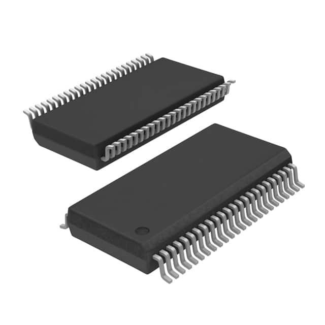
The 74LVC16241ADL,118 is available in a small-outline package (SO) with 48 pins.
Essence
The essence of this product lies in its ability to provide reliable signal buffering and driving capabilities for digital circuits.
Packaging/Quantity
The 74LVC16241ADL,118 is typically packaged in reels or tubes, with a quantity of 2500 units per reel/tube.
Specifications
- Supply voltage: 1.2V to 3.6V
- Input voltage range: 0V to VCC
- Output voltage range: 0V to VCC
- Operating temperature range: -40°C to +85°C
- Maximum input current: ±24mA
- Maximum output current: ±32mA
Detailed Pin Configuration
The 74LVC16241ADL,118 has a total of 48 pins, which are divided into four groups of twelve pins each. The pin configuration is as follows:
Group A: 1. OE1 (Output Enable Input 1) 2. I/O1A (Input/Output 1A) 3. I/O1B (Input/Output 1B) 4. GND (Ground) 5. I/O1C (Input/Output 1C) 6. I/O1D (Input/Output 1D) 7. VCC (Supply Voltage) 8. I/O1E (Input/Output 1E) 9. I/O1F (Input/Output 1F) 10. GND (Ground) 11. I/O1G (Input/Output 1G) 12. I/O1H (Input/Output 1H)
Group B, C, and D have similar pin configurations.
Functional Features
- Buffering: The 74LVC16241ADL,118 provides buffering capabilities to ensure signal integrity and prevent signal degradation.
- Line Driving: It can drive signals over long distances without significant loss or distortion.
- Schmitt-trigger Action: The Schmitt-trigger action on all inputs helps in noise immunity and provides hysteresis for better signal stability.
- Balanced Propagation Delays: The IC ensures balanced propagation delays across all outputs, maintaining synchronization between multiple signals.
Advantages and Disadvantages
Advantages
- Low voltage operation allows compatibility with a wide range of digital systems.
- High-speed operation enables efficient data transfer.
- Schmitt-trigger action enhances noise immunity.
- Symmetrical output impedance simplifies circuit design.
Disadvantages
- Limited output current may restrict its use in certain high-power applications.
- Availability of alternative models with additional features may limit its competitiveness in the market.
Working Principles
The 74LVC16241ADL,118 operates based on CMOS technology. It uses a combination of transistors to amplify and buffer digital signals. When an input signal is received, the IC amplifies it and drives the output with minimal delay and distortion. The Schmitt-trigger action ensures stable output transitions even in the presence of noise.
Detailed Application Field Plans
The 74LVC16241ADL,118 finds applications in various digital systems, including: - Microcontrollers - Data communication systems - Memory interfaces - Industrial automation - Automotive electronics
Detailed and Complete Alternative Models
- 74LVC16244A: Similar to the 74LVC16241ADL,118 but with inverted outputs.
- 74LVCH16245A: Offers higher output current capability for more demanding applications.
- 74LVC16245A: Provides bidirectional level shifting capabilities in addition to buffering.
These alternative models offer similar functionality with slight variations to cater to specific requirements.
In conclusion, the 74LVC16241ADL,118 is a versatile integrated circuit that serves as a buffer/line driver for digital applications. Its low voltage operation, high-speed performance, and Schmitt-trigger action make it suitable for various digital systems. While it has certain limitations, alternative models are available to address specific needs.
قم بإدراج 10 أسئلة وإجابات شائعة تتعلق بتطبيق 74LVC16241ADL,118 في الحلول التقنية
Sure! Here are 10 common questions and answers related to the application of 74LVC16241ADL,118:
Q: What is the 74LVC16241ADL,118? A: The 74LVC16241ADL,118 is a 16-bit buffer/driver with 3-state outputs. It is designed for low-voltage (2.5V to 3.6V) applications.
Q: What is the purpose of the 74LVC16241ADL,118? A: The purpose of this IC is to provide buffering and driving capabilities for digital signals in various electronic circuits.
Q: What voltage levels does the 74LVC16241ADL,118 support? A: The 74LVC16241ADL,118 supports voltage levels between 2.5V and 3.6V.
Q: How many inputs and outputs does the 74LVC16241ADL,118 have? A: This IC has 16 inputs and 16 outputs.
Q: Can the 74LVC16241ADL,118 be used for bidirectional communication? A: No, the 74LVC16241ADL,118 is a unidirectional buffer/driver and does not support bidirectional communication.
Q: What is the maximum output current of the 74LVC16241ADL,118? A: The maximum output current per channel is typically 32mA.
Q: Can the 74LVC16241ADL,118 handle high-speed signals? A: Yes, this IC is designed for high-speed operation and can handle signals with fast rise and fall times.
Q: Is the 74LVC16241ADL,118 compatible with TTL and CMOS logic levels? A: Yes, this IC is compatible with both TTL and CMOS logic levels.
Q: Can the 74LVC16241ADL,118 be used in automotive applications? A: Yes, the 74LVC16241ADL,118 is qualified for automotive applications and meets the necessary standards.
Q: Are there any specific precautions to consider when using the 74LVC16241ADL,118? A: It is important to follow the recommended operating conditions, such as voltage levels and temperature ranges, specified in the datasheet. Additionally, proper decoupling capacitors should be used to ensure stable operation.