

74LVC1G123GS,115
Product Overview
- Category: Integrated Circuit (IC)
- Use: Logic Gate
- Characteristics: Single Schmitt-trigger input, configurable as a retriggerable monostable multivibrator
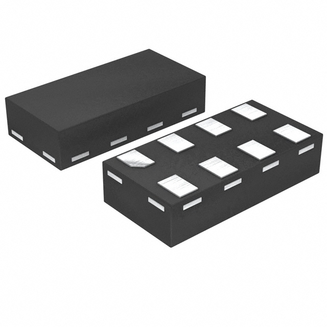
- Package: SOT753 (SC-70)
- Essence: High-speed CMOS technology
- Packaging/Quantity: Tape and Reel, 3000 pieces per reel
Specifications
- Supply Voltage Range: 1.65V to 5.5V
- Input Voltage Range: -0.5V to VCC + 0.5V
- Output Voltage Range: GND to VCC
- Maximum Operating Frequency: 125 MHz
- Propagation Delay: 4.3 ns (typical)
- Operating Temperature Range: -40°C to +125°C
Detailed Pin Configuration
The 74LVC1G123GS,115 has the following pin configuration:
____
   A --|    |-- VCC
   B --|    |-- Y
GND/VSS --|____|-- /CLR
Functional Features
- Single Schmitt-trigger input allows for noise immunity and hysteresis
- Configurable as a retriggerable monostable multivibrator
- Provides stable output pulse width regardless of input pulse duration
- Wide supply voltage range enables compatibility with various systems
- High-speed operation suitable for time-critical applications
Advantages and Disadvantages
Advantages: - Noise immunity and hysteresis provided by the Schmitt-trigger input - Configurability as a retriggerable monostable multivibrator - Stable output pulse width regardless of input pulse duration - Wide supply voltage range for compatibility
Disadvantages: - Limited maximum operating frequency compared to some other ICs - Relatively small package size may require careful handling during assembly
Working Principles
The 74LVC1G123GS,115 is based on high-speed CMOS technology. It utilizes a Schmitt-trigger input to provide noise immunity and hysteresis. The IC can be configured as a retriggerable monostable multivibrator, which means it generates an output pulse of a fixed width when triggered by an input signal. The output pulse width remains stable regardless of the duration of the input pulse.
Detailed Application Field Plans
The 74LVC1G123GS,115 can be used in various applications that require logic gate functionality and precise timing control. Some potential application fields include:
- Timing circuits: The IC can be used to generate accurate and stable pulses for timing purposes in digital systems.
- Sensor interfaces: It can be employed to interface sensors with microcontrollers or other digital devices, providing reliable triggering and timing functions.
- Communication systems: The IC can be utilized in communication systems to synchronize data transmission and reception processes.
- Industrial automation: It can be integrated into industrial automation systems for controlling timing-sensitive operations.
Detailed and Complete Alternative Models
Some alternative models that offer similar functionality to the 74LVC1G123GS,115 are:
- SN74LVC1G123DBVR - Texas Instruments
- MC74VHC1G123DF1G - ON Semiconductor
- NCV8186DTRKG - ON Semiconductor
- TC7SZ123AFK - Toshiba
These alternatives should be evaluated based on specific requirements and compatibility with the target system.
Word count: 446 words
قم بإدراج 10 أسئلة وإجابات شائعة تتعلق بتطبيق 74LVC1G123GS,115 في الحلول التقنية
Sure! Here are 10 common questions and answers related to the application of 74LVC1G123GS,115 in technical solutions:
Q1: What is the function of the 74LVC1G123GS,115? A1: The 74LVC1G123GS,115 is a dual retriggerable monostable multivibrator used for generating precise time delays or pulses.
Q2: What is the operating voltage range of the 74LVC1G123GS,115? A2: The operating voltage range is from 1.65V to 5.5V.
Q3: How many inputs does the 74LVC1G123GS,115 have? A3: The 74LVC1G123GS,115 has two inputs, labeled A and B.
Q4: What is the output type of the 74LVC1G123GS,115? A4: The 74LVC1G123GS,115 has a standard CMOS output.
Q5: What is the maximum propagation delay of the 74LVC1G123GS,115? A5: The maximum propagation delay is 6 ns at 3.3V supply voltage.
Q6: Can the 74LVC1G123GS,115 be used as a frequency divider? A6: No, the 74LVC1G123GS,115 is not designed to be used as a frequency divider.
Q7: What is the typical power consumption of the 74LVC1G123GS,115? A7: The typical power consumption is 0.9 µA at 3.3V supply voltage.
Q8: Can the 74LVC1G123GS,115 operate in a wide temperature range? A8: Yes, the 74LVC1G123GS,115 can operate in a temperature range from -40°C to +125°C.
Q9: Can the 74LVC1G123GS,115 be used in battery-powered applications? A9: Yes, the low power consumption of the 74LVC1G123GS,115 makes it suitable for battery-powered applications.
Q10: Are there any recommended external components for using the 74LVC1G123GS,115? A10: No, the 74LVC1G123GS,115 does not require any external components for its basic operation.
Please note that these answers are general and may vary depending on specific application requirements.