

74LVC1G57GV-Q100H
Product Overview
- Category: Logic ICs
- Use: Voltage Level Translator
- Characteristics: Low-Voltage CMOS, Single Gate, Non-Inverting Buffer/Translator
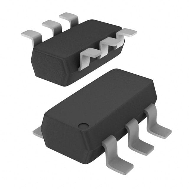
- Package: SOT753 (SC-70)
- Essence: This product is a single gate voltage level translator designed for low-voltage applications.
- Packaging/Quantity: Available in tape and reel packaging with 3000 units per reel.
Specifications
- Supply Voltage Range: 1.65V to 5.5V
- Input Voltage Range: GND to VCC
- Output Voltage Range: GND to VCC
- High-Level Input Voltage: 0.7 x VCC to VCC + 0.3V
- Low-Level Input Voltage: GND to 0.3 x VCC
- High-Level Output Voltage: 0.9 x VCC to VCC
- Low-Level Output Voltage: GND to 0.1 x VCC
- Propagation Delay: 4.2 ns (typical)
- Operating Temperature Range: -40°C to +125°C
Detailed Pin Configuration
The 74LVC1G57GV-Q100H has the following pin configuration:
____
   A1 |    | VCC
   B1 |    | Y1
   GND |____| A2
        ____
   B2  |    |
   Y2  |    |
   GND |____|
Functional Features
- Provides non-inverting voltage level translation between different logic levels.
- Supports bidirectional voltage translation.
- Wide operating voltage range allows compatibility with various systems.
- High-speed operation with low propagation delay.
- Low power consumption.
- Schmitt-trigger input allows for better noise immunity.
Advantages
- Small package size enables space-saving designs.
- Wide supply voltage range makes it versatile for different applications.
- High-speed operation enhances system performance.
- Low power consumption helps in reducing overall energy consumption.
- Schmitt-trigger input ensures reliable operation even in noisy environments.
Disadvantages
- Limited number of translation channels (single gate).
- Not suitable for high-voltage applications.
- May require additional external components for certain applications.
Working Principles
The 74LVC1G57GV-Q100H is a voltage level translator that uses CMOS technology. It operates by receiving an input signal at one logic level and translating it to another logic level. The device consists of a single gate that performs the level translation function. It utilizes a combination of MOSFETs and control circuitry to achieve the desired voltage translation.
Detailed Application Field Plans
The 74LVC1G57GV-Q100H can be used in various applications, including:
- Battery-powered devices: Due to its low power consumption and wide operating voltage range, it is suitable for portable electronics such as smartphones, tablets, and wearables.
- Industrial automation: Can be used in control systems, sensors, and actuators where voltage level translation is required.
- Automotive electronics: Suitable for automotive applications that involve voltage translation between different subsystems or components.
- Communication systems: Can be used in networking equipment, routers, and switches for voltage level translation between different logic families.
Detailed and Complete Alternative Models
- SN74LVC1G57DBVR - Single Gate Non-Inverting Buffer/Translator, SOT23-5 Package
- NC7SZ57P6X - Single Gate Non-Inverting Buffer/Translator, SC-70 Package
- TC7SZ57FU - Single Gate Non-Inverting Buffer/Translator, SOT353 Package
- 74LVC1G57GW - Single Gate Non-Inverting Buffer/Translator, SOT323-5 Package
These alternative models offer similar functionality and can be considered as alternatives to the 74LVC1G57GV-Q100H.
In conclusion, the 74LVC1G57GV-Q100H is a single gate voltage level translator that provides non-inverting translation between different logic levels. It offers advantages such as small package size, wide supply voltage range, high-speed operation, and low power consumption. However, it has limitations in terms of the number of translation channels and suitability for high-voltage applications. It finds applications in battery-powered devices, industrial automation, automotive electronics, and communication systems. Alternative models with similar functionality are also available in the market.
قم بإدراج 10 أسئلة وإجابات شائعة تتعلق بتطبيق 74LVC1G57GV-Q100H في الحلول التقنية
Sure! Here are 10 common questions and answers related to the application of 74LVC1G57GV-Q100H in technical solutions:
Q1: What is the 74LVC1G57GV-Q100H? A1: The 74LVC1G57GV-Q100H is a single-pole, double-throw (SPDT) analog switch designed for low-voltage applications.
Q2: What is the voltage range supported by the 74LVC1G57GV-Q100H? A2: The 74LVC1G57GV-Q100H supports a voltage range from 1.65V to 5.5V.
Q3: What is the maximum current rating of the 74LVC1G57GV-Q100H? A3: The 74LVC1G57GV-Q100H has a maximum current rating of 32mA.
Q4: Can the 74LVC1G57GV-Q100H be used for bidirectional signal switching? A4: Yes, the 74LVC1G57GV-Q100H can be used for bidirectional signal switching.
Q5: What is the typical on-resistance of the 74LVC1G57GV-Q100H? A5: The typical on-resistance of the 74LVC1G57GV-Q100H is around 6 ohms.
Q6: Is the 74LVC1G57GV-Q100H suitable for high-speed applications? A6: Yes, the 74LVC1G57GV-Q100H is suitable for high-speed applications with a propagation delay of typically 2.5ns.
Q7: Can the 74LVC1G57GV-Q100H handle both analog and digital signals? A7: Yes, the 74LVC1G57GV-Q100H can handle both analog and digital signals.
Q8: What is the package type of the 74LVC1G57GV-Q100H? A8: The 74LVC1G57GV-Q100H is available in a small SOT-353 package.
Q9: Does the 74LVC1G57GV-Q100H have built-in ESD protection? A9: Yes, the 74LVC1G57GV-Q100H has built-in ESD protection up to 2kV.
Q10: Can the 74LVC1G57GV-Q100H be used in automotive applications? A10: Yes, the 74LVC1G57GV-Q100H is qualified for automotive applications and meets the AEC-Q100 standard.
Please note that these answers are general and may vary depending on the specific datasheet and manufacturer's specifications.