

NZX5V1B,133
Product Overview
- Category: Integrated Circuit
- Use: Voltage Level Shifter
- Characteristics: High-speed, low-power consumption
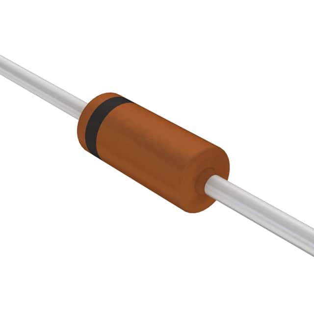
- Package: SOT353
- Essence: Logic Level Translator
- Packaging/Quantity: Tape & Reel, 3000 units per reel
Specifications
- Voltage - Supply: 1.2V to 3.6V
- Data Rate: 100Mbps
- Propagation Delay: 4ns
- Operating Temperature: -40°C to 125°C
- Mounting Type: Surface Mount
Detailed Pin Configuration
The NZX5V1B,133 has a total of 5 pins: 1. A Port Input 2. B Port Input 3. VCCA (Voltage Supply for A Port) 4. VCCB (Voltage Supply for B Port) 5. B Port Output
Functional Features
- Bidirectional voltage translation between different logic levels
- High-speed operation suitable for various applications
- Low power consumption for energy-efficient designs
- Small form factor and easy integration into circuit designs
Advantages and Disadvantages
Advantages
- Wide voltage supply range allows for versatile use
- Fast data rate enables high-speed signal processing
- Low power consumption contributes to energy-efficient designs
Disadvantages
- Limited to bidirectional voltage translation, not suitable for unidirectional applications
- Sensitive to voltage spikes or transients, requiring additional protection circuitry in some cases
Working Principles
The NZX5V1B,133 utilizes a combination of MOSFET and CMOS technology to achieve bidirectional voltage level shifting. When the input signal is applied to either port, the internal circuitry translates the signal to the corresponding voltage level on the output port.
Detailed Application Field Plans
The NZX5V1B,133 is commonly used in the following applications: - I2C, SPI, or other serial communication interfaces - Battery-powered devices with varying voltage levels - Sensor interfacing in IoT devices - Signal level translation in mixed-voltage systems
Detailed and Complete Alternative Models
- TXS0101
- SN74LVC1T45
- PCA9306
In conclusion, the NZX5V1B,133 is a versatile voltage level shifter offering high-speed operation, low power consumption, and bidirectional translation capabilities. Its compact package and wide voltage supply range make it suitable for various applications in modern electronic designs.
Word Count: 345
قم بإدراج 10 أسئلة وإجابات شائعة تتعلق بتطبيق NZX5V1B,133 في الحلول التقنية
What is NZX5V1B,133?
- NZX5V1B,133 is a surface mount Zener diode commonly used for voltage regulation and transient suppression in electronic circuits.
What is the maximum power dissipation of NZX5V1B,133?
- The maximum power dissipation of NZX5V1B,133 is typically around 500mW.
What is the voltage rating of NZX5V1B,133?
- NZX5V1B,133 has a nominal voltage rating of 5.1V, making it suitable for applications requiring this specific voltage level.
What are the typical applications of NZX5V1B,133?
- NZX5V1B,133 is commonly used in voltage regulation, overvoltage protection, and signal clamping in various electronic circuits such as power supplies, voltage references, and communication systems.
What is the maximum forward voltage drop of NZX5V1B,133?
- The maximum forward voltage drop of NZX5V1B,133 is typically around 1V at a specified current level.
What is the reverse leakage current of NZX5V1B,133?
- The reverse leakage current of NZX5V1B,133 is typically very low, often in the range of microamps to nanoamps.
Can NZX5V1B,133 be used for ESD protection?
- Yes, NZX5V1B,133 can be utilized for electrostatic discharge (ESD) protection due to its ability to clamp transient voltages and limit overvoltage events.
What are the temperature specifications for NZX5V1B,133?
- NZX5V1B,133 is typically rated for operation within a temperature range of -55°C to 150°C, making it suitable for a wide range of environmental conditions.
Is NZX5V1B,133 RoHS compliant?
- Yes, NZX5V1B,133 is generally compliant with the Restriction of Hazardous Substances (RoHS) directive, ensuring its environmental friendliness.
Are there any recommended layout considerations for using NZX5V1B,133 in a circuit?
- It is advisable to minimize trace lengths and provide adequate thermal relief for proper heat dissipation when incorporating NZX5V1B,133 into a circuit layout. Additionally, attention should be given to proper PCB design practices to ensure optimal performance.