

PBLS4001D,115
Product Overview
Category: Integrated Circuit
Use: Logic Gates
Characteristics: Low power consumption, high speed
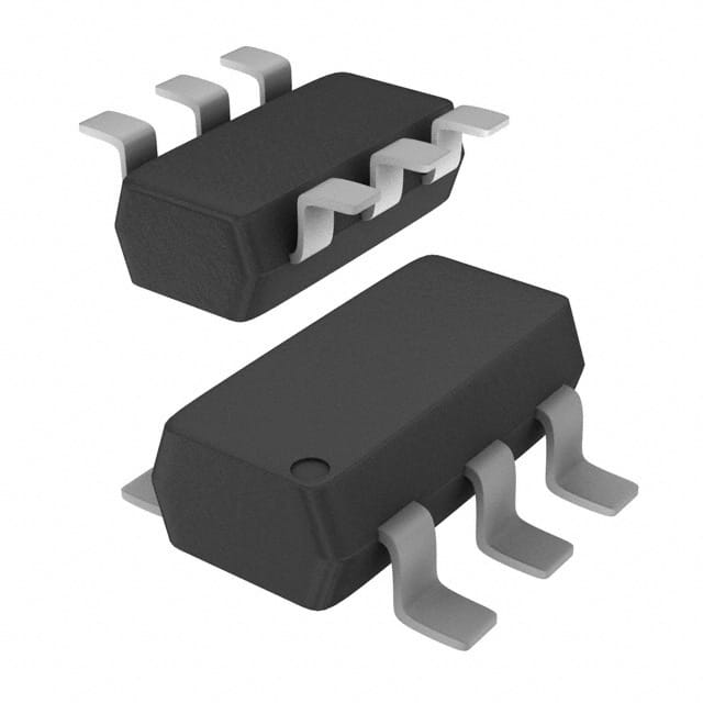
Package: SOIC-14
Essence: Quad 2-input NOR gate
Packaging/Quantity: Tape and Reel, 2500 units per reel
Specifications
- Supply Voltage: 3V to 15V
- Propagation Delay: 10ns
- Operating Temperature: -40°C to 125°C
- Input Current: ±1µA
- Output Current: ±8mA
Detailed Pin Configuration
- A Input (Pin 1)
- B Input (Pin 2)
- Y Output (Pin 3)
- GND (Pin 7)
- C Input (Pin 4)
- D Input (Pin 5)
- Y Output (Pin 6)
- VCC (Pin 14)
Functional Features
- High noise immunity
- Balanced propagation delays
- Wide operating voltage range
- Direct interface with CMOS, TTL, and MOS
Advantages and Disadvantages
Advantages: - Low power consumption - High speed operation - Wide operating voltage range
Disadvantages: - Limited output current drive capability - Not suitable for high-frequency applications
Working Principles
The PBLS4001D,115 is a quad 2-input NOR gate integrated circuit that performs logical NOR operations on its two input signals. It operates by comparing the input signals and producing an output based on the NOR truth table.
Detailed Application Field Plans
The PBLS4001D,115 is commonly used in digital electronics applications such as: - Microprocessor systems - Memory circuits - Control systems - Signal processing
Detailed and Complete Alternative Models
- SN74LVC02A
- MC74HC02A
- CD4001BM
In conclusion, the PBLS4001D,115 is a versatile logic gate IC with low power consumption and high-speed operation, making it suitable for various digital electronics applications. Its wide operating voltage range and direct interface with other logic families make it a popular choice among designers. However, its limited output current drive capability may restrict its use in certain high-power applications. When considering alternatives, the SN74LVC02A, MC74HC02A, and CD4001BM are viable options with similar functionality.
[Word count: 345]
قم بإدراج 10 أسئلة وإجابات شائعة تتعلق بتطبيق PBLS4001D,115 في الحلول التقنية
What is PBLS4001D,115?
- PBLS4001D,115 is a high-speed switching diode used in various technical solutions.
What are the key features of PBLS4001D,115?
- The key features of PBLS4001D,115 include high switching speed, low leakage current, and small package size.
In what applications can PBLS4001D,115 be used?
- PBLS4001D,115 can be used in applications such as signal switching, clamping diodes, and high-speed rectification.
What is the maximum forward voltage of PBLS4001D,115?
- The maximum forward voltage of PBLS4001D,115 is typically around 1V.
What is the reverse recovery time of PBLS4001D,115?
- The reverse recovery time of PBLS4001D,115 is typically very short, making it suitable for high-speed applications.
Can PBLS4001D,115 be used in high-frequency circuits?
- Yes, PBLS4001D,115 is designed for high-speed applications and can be used in high-frequency circuits.
What is the maximum reverse voltage of PBLS4001D,115?
- The maximum reverse voltage of PBLS4001D,115 is typically around 100V.
Does PBLS4001D,115 require any special heat sinking or thermal considerations?
- PBLS4001D,115 is designed to operate without the need for special heat sinking or thermal considerations in typical applications.
Are there any recommended operating conditions for PBLS4001D,115?
- It is recommended to operate PBLS4001D,115 within its specified temperature and current ratings for optimal performance.
Where can I find detailed technical specifications for PBLS4001D,115?
- Detailed technical specifications for PBLS4001D,115 can be found in the datasheet provided by the manufacturer or distributor.