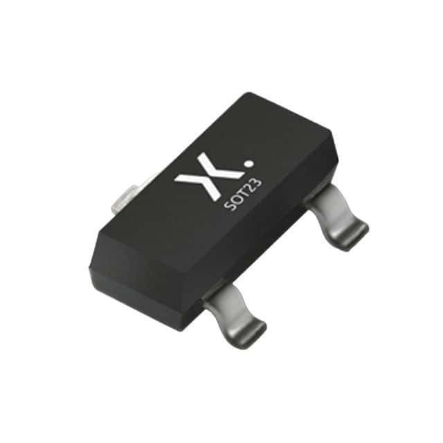
PDTA113ET,215
Product Category: Transistor
Basic Information Overview: - Category: NPN Bipolar Transistor - Use: Amplification and Switching - Characteristics: High voltage, low current, small package size - Package: SOT416 (SC-75) - Essence: Small signal transistor for general purpose applications - Packaging/Quantity: Tape and Reel, 3000 units per reel
Specifications: - Collector-Base Voltage (VCBO): 50V - Collector-Emitter Voltage (VCEO): 50V - Emitter-Base Voltage (VEBO): 5V - Collector Current (IC): 100mA - Total Power Dissipation (PTOT): 250mW - Transition Frequency (fT): 200MHz - Operating Temperature Range (Tj): -55°C to +150°C
Detailed Pin Configuration: - Pin 1 (Emitter) - Pin 2 (Base) - Pin 3 (Collector)
Functional Features: - High voltage capability - Low leakage current - Fast switching speed - Small package size
Advantages: - Suitable for high voltage applications - Compact and space-saving design - Wide operating temperature range
Disadvantages: - Limited collector current compared to some alternatives - Sensitive to static electricity due to small package size
Working Principles: The PDTA113ET,215 operates based on the principles of bipolar junction transistors, utilizing the flow of charge carriers to amplify or switch electronic signals.
Detailed Application Field Plans: - Audio amplification circuits - Signal processing circuits - Switching circuits in portable devices
Detailed and Complete Alternative Models: - BC847B,215 - MMBT3904LT1G - 2N3904
This comprehensive entry provides a detailed overview of the PDTA113ET,215, covering its category, basic information, specifications, pin configuration, functional features, advantages and disadvantages, working principles, application field plans, and alternative models.
قم بإدراج 10 أسئلة وإجابات شائعة تتعلق بتطبيق PDTA113ET,215 في الحلول التقنية
What is PDTA113ET,215?
- PDTA113ET,215 is a NPN resistor-equipped transistor designed for use in general-purpose amplifier and switching applications.
What are the key features of PDTA113ET,215?
- The key features of PDTA113ET,215 include its high current gain, low collector-emitter saturation voltage, and built-in resistor for biasing.
What are the typical applications of PDTA113ET,215?
- Typical applications of PDTA113ET,215 include audio amplification, signal processing, and general switching circuits.
What is the maximum collector current of PDTA113ET,215?
- The maximum collector current of PDTA113ET,215 is 100mA.
What is the maximum power dissipation of PDTA113ET,215?
- The maximum power dissipation of PDTA113ET,215 is 200mW.
What is the voltage rating for PDTA113ET,215?
- The voltage rating for PDTA113ET,215 is 50V.
What is the thermal resistance of PDTA113ET,215?
- The thermal resistance of PDTA113ET,215 is typically 625°C/W.
What are the recommended operating conditions for PDTA113ET,215?
- The recommended operating conditions for PDTA113ET,215 include a collector current of 10mA to 100mA and a collector-emitter voltage of 45V.
Can PDTA113ET,215 be used in high-frequency applications?
- No, PDTA113ET,215 is not suitable for high-frequency applications due to its limited frequency response.
Are there any specific layout considerations when using PDTA113ET,215 in a circuit?
- It is recommended to minimize the length of the connections to PDTA113ET,215 and provide adequate heat sinking if operating at high currents or power levels.


