

NX3DV2567HR-Q100X
Product Overview
- Category: Integrated Circuit (IC)
- Use: Digital Multiplexer/Demultiplexer
- Characteristics: High-speed, Low-power, Wide voltage range
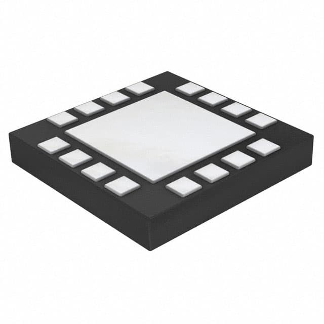
- Package: QFN (Quad Flat No-leads)
- Essence: Advanced digital signal processing technology
- Packaging/Quantity: Tape and Reel, 2500 units per reel
Specifications
- Number of Channels: 16
- Supply Voltage Range: 1.65V to 5.5V
- Operating Temperature Range: -40°C to +125°C
- Input Capacitance: 2pF (typical)
- On-state Resistance: 4Ω (typical)
- Propagation Delay Time: 0.8ns (typical)
Detailed Pin Configuration
The NX3DV2567HR-Q100X has a total of 24 pins. The pin configuration is as follows:
- VCC
- Channel 0 Input
- Channel 1 Input
- Channel 2 Input
- Channel 3 Input
- Channel 4 Input
- Channel 5 Input
- Channel 6 Input
- Channel 7 Input
- Channel 8 Input
- Channel 9 Input
- Channel 10 Input
- Channel 11 Input
- Channel 12 Input
- Channel 13 Input
- Channel 14 Input
- Channel 15 Input
- GND
- Enable Input
- Channel Select Input
- Channel 0 Output
- Channel 1 Output
- Channel 2 Output
- Channel 3 Output
Functional Features
- High-speed switching between channels
- Low power consumption
- Wide voltage range compatibility
- ESD protection on all pins
- Break-before-make switching
Advantages and Disadvantages
Advantages: - Fast signal processing - Low power consumption - Wide voltage range compatibility - ESD protection for enhanced reliability - Break-before-make switching prevents short circuits
Disadvantages: - Limited number of channels (16) - Relatively high input capacitance
Working Principles
The NX3DV2567HR-Q100X is a digital multiplexer/demultiplexer IC that allows the selection of one input channel from multiple inputs to be routed to an output channel. It operates based on advanced digital signal processing technology, enabling high-speed switching between channels with minimal propagation delay.
The IC is designed to work within a wide voltage range, making it suitable for various applications. It consumes low power, making it energy-efficient. The device also provides ESD protection on all pins, ensuring enhanced reliability in harsh environments.
The break-before-make switching mechanism ensures that there is no short circuit during the transition between channels, further improving the overall performance and safety of the IC.
Detailed Application Field Plans
The NX3DV2567HR-Q100X finds applications in various fields, including:
- Communication Systems: Used for signal routing and switching in telecommunication networks.
- Data Acquisition Systems: Enables the selection of specific data sources for processing or analysis.
- Test and Measurement Equipment: Allows the routing of test signals to different measurement instruments.
- Audio/Video Switching: Used in audio/video systems to select different sources for display or playback.
- Industrial Automation: Enables the control of different sensors or actuators in automated systems.
Detailed and Complete Alternative Models
- SN74LV4051A: 8-channel analog multiplexer/demultiplexer IC.
- CD74HC4067: 16-channel analog multiplexer/demultiplexer IC.
- ADG732: 32-channel digital multiplexer/demultiplexer IC.
These alternative models offer similar functionality and can be considered as alternatives to the NX3DV2567HR-Q100X based on specific requirements and application needs.
Word count: 410 words
قم بإدراج 10 أسئلة وإجابات شائعة تتعلق بتطبيق NX3DV2567HR-Q100X في الحلول التقنية
Sure! Here are 10 common questions and answers related to the application of NX3DV2567HR-Q100X in technical solutions:
Q: What is the NX3DV2567HR-Q100X? A: The NX3DV2567HR-Q100X is a high-speed, low-power, bidirectional voltage level translator IC.
Q: What is the voltage range supported by the NX3DV2567HR-Q100X? A: The NX3DV2567HR-Q100X supports voltage translation from 1.2V to 3.6V.
Q: How many channels does the NX3DV2567HR-Q100X have? A: The NX3DV2567HR-Q100X has 8 channels for bidirectional voltage translation.
Q: What is the maximum data rate supported by the NX3DV2567HR-Q100X? A: The NX3DV2567HR-Q100X supports data rates up to 400 Mbps.
Q: Can the NX3DV2567HR-Q100X be used in both uni-directional and bi-directional applications? A: Yes, the NX3DV2567HR-Q100X can be used in both uni-directional and bi-directional applications.
Q: What is the power supply voltage required for the NX3DV2567HR-Q100X? A: The NX3DV2567HR-Q100X requires a power supply voltage of 1.65V to 3.6V.
Q: Does the NX3DV2567HR-Q100X support hot-swapping? A: Yes, the NX3DV2567HR-Q100X supports hot-swapping, allowing for easy insertion and removal of devices.
Q: Can the NX3DV2567HR-Q100X be used in automotive applications? A: Yes, the NX3DV2567HR-Q100X is qualified for automotive applications and meets the AEC-Q100 standard.
Q: What is the package type of the NX3DV2567HR-Q100X? A: The NX3DV2567HR-Q100X is available in a 20-pin VQFN package.
Q: Are there any evaluation boards or reference designs available for the NX3DV2567HR-Q100X? A: Yes, NXP provides evaluation boards and reference designs to help with the implementation of the NX3DV2567HR-Q100X in various applications.
Please note that these answers are general and may vary depending on the specific requirements and use cases. It's always recommended to refer to the datasheet and application notes provided by the manufacturer for detailed information.