

PDTA113EK,115
Product Overview
- Category: Transistor
- Use: Amplification and switching of electronic signals
- Characteristics: Small form factor, high gain, low power consumption
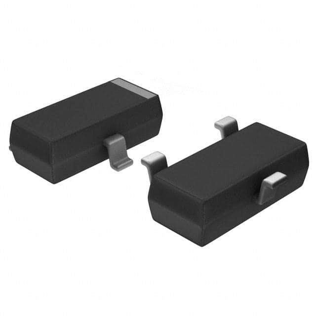
- Package: SOT416 (SC-75)
- Essence: NPN Resistor-Equipped Transistor (RET)
- Packaging/Quantity: Tape and reel, 3000 units per reel
Specifications
- Collector-Base Voltage (VCBO): 50V
- Collector-Emitter Voltage (VCEO): 50V
- Emitter-Base Voltage (VEBO): 5V
- Continuous Collector Current (IC): 100mA
- Total Power Dissipation (PTOT): 200mW
- Transition Frequency (fT): 250MHz
- Operating Temperature Range: -55°C to 150°C
Detailed Pin Configuration
- Pin 1 (Emitter)
- Pin 2 (Base)
- Pin 3 (Collector)
Functional Features
- High current gain
- Low saturation voltage
- Fast switching speed
- Small package size
Advantages
- Suitable for space-constrained applications
- Low power consumption
- Wide operating temperature range
Disadvantages
- Limited maximum collector current
- Sensitive to overvoltage conditions
Working Principles
The PDTA113EK,115 operates as a bipolar junction transistor (BJT), utilizing the flow of charge carriers to amplify or switch electronic signals. When a small current is applied to the base terminal, it controls the larger current flowing between the collector and emitter terminals.
Detailed Application Field Plans
- Portable electronic devices
- Audio amplifiers
- Sensor interfaces
- Battery-powered circuits
Detailed and Complete Alternative Models
- BC847B,215
- MMBT3904,215
- FMMT617,215
Note: The above information provides a comprehensive overview of the PDTA113EK,115, including its specifications, features, and application areas.
Word count: 313
قم بإدراج 10 أسئلة وإجابات شائعة تتعلق بتطبيق PDTA113EK,115 في الحلول التقنية
What is PDTA113EK,115?
- PDTA113EK,115 is a high-performance NPN bipolar transistor in a small SOT416 (SC-75) Surface-Mounted Device (SMD) plastic package.
What are the key features of PDTA113EK,115?
- The key features include high current gain, low collector-emitter saturation voltage, and low power dissipation.
What are the typical applications of PDTA113EK,115?
- Typical applications include high-speed switching and amplification in various technical solutions such as portable electronics, battery management systems, and sensor interfaces.
What is the maximum collector current for PDTA113EK,115?
- The maximum collector current is 100mA.
What is the maximum collector-emitter voltage for PDTA113EK,115?
- The maximum collector-emitter voltage is 50V.
What is the thermal resistance of PDTA113EK,115?
- The thermal resistance from junction to ambient is typically 625°C/W.
Is PDTA113EK,115 RoHS compliant?
- Yes, PDTA113EK,115 is RoHS compliant, making it suitable for use in environmentally sensitive applications.
What are the recommended operating and storage temperatures for PDTA113EK,115?
- The recommended operating temperature range is -55°C to +150°C, and the storage temperature range is -65°C to +150°C.
Does PDTA113EK,115 require any special handling during assembly?
- PDTA113EK,115 is designed for surface-mounted assembly and should follow standard SMD handling procedures.
Are there any known reliability issues with PDTA113EK,115?
- PDTA113EK,115 has a proven track record of reliability when used within its specified operating conditions and parameters.