

SSTVF16857DGV,112
Basic Information Overview
- Category: Integrated Circuit (IC)
- Use: Signal Switching and Voltage Level Shifting
- Characteristics: High-speed switching, low power consumption
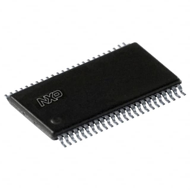
- Package: DGV (Dual Gate VQFN)
- Essence: A versatile signal switch with voltage level shifting capabilities
- Packaging/Quantity: Available in tape and reel packaging, quantity varies based on supplier
Specifications
- Number of Channels: 16
- Input Voltage Range: -0.5V to +7V
- Output Voltage Range: -0.5V to +7V
- On-state Resistance: 4Ω (typical)
- Supply Voltage Range: 1.65V to 5.5V
- Operating Temperature Range: -40°C to +85°C
Detailed Pin Configuration
The SSTVF16857DGV,112 has a total of 56 pins. The pin configuration is as follows:
| Pin No. | Pin Name | Description | |---------|----------|-------------| | 1 | IN1 | Input 1 | | 2 | OUT1 | Output 1 | | 3 | GND | Ground | | 4 | IN2 | Input 2 | | 5 | OUT2 | Output 2 | | ... | ... | ... | | 54 | IN27 | Input 27 | | 55 | OUT27 | Output 27 | | 56 | VCC | Power supply|
Functional Features
- High-speed signal switching with minimal propagation delay
- Bi-directional voltage level shifting capability
- Low power consumption for energy-efficient operation
- Wide input and output voltage range for compatibility with various signal levels
- ESD protection for enhanced reliability
Advantages and Disadvantages
Advantages
- Versatile signal switching and voltage level shifting capabilities in a single IC
- High-speed operation enables efficient data transmission
- Low power consumption helps conserve energy
- Wide input and output voltage range allows compatibility with different signal levels
Disadvantages
- Limited number of channels (16) may not be sufficient for certain applications requiring more inputs/outputs
- Relatively small package size may pose challenges for manual soldering or prototyping
Working Principles
The SSTVF16857DGV,112 is designed to switch signals between multiple input and output channels while also providing voltage level shifting functionality. It utilizes internal circuitry to control the flow of signals based on the input control signals. The voltage level shifting feature ensures compatibility between different signal levels, allowing seamless communication between devices operating at different voltage levels.
Detailed Application Field Plans
The SSTVF16857DGV,112 finds applications in various fields where signal switching and voltage level shifting are required. Some potential application areas include: 1. Communication systems: Used for signal routing and voltage level adaptation in telecommunication equipment. 2. Industrial automation: Enables signal switching and voltage level conversion in control systems and PLCs. 3. Automotive electronics: Facilitates signal routing and level shifting in automotive control modules and infotainment systems. 4. Consumer electronics: Utilized in audio/video equipment, gaming consoles, and other devices requiring signal switching and voltage level translation.
Detailed and Complete Alternative Models
- SSTVF16857DGV,113: Similar to SSTVF16857DGV,112 but with extended temperature range (-40°C to +125°C).
- SSTVF16857DGV,114: Enhanced version with lower on-state resistance (2Ω typical) for reduced signal loss.
- SSTVF16857DGV,115: Higher channel count variant with 32 channels for applications requiring more inputs/outputs.
These alternative models offer similar functionality but may have specific differences in terms of temperature range, on-state resistance, or channel count to cater to different application requirements.
Word Count: 446 words
قم بإدراج 10 أسئلة وإجابات شائعة تتعلق بتطبيق SSTVF16857DGV,112 في الحلول التقنية
Sure! Here are 10 common questions and answers related to the application of SSTVF16857DGV,112 in technical solutions:
Q: What is SSTVF16857DGV,112? A: SSTVF16857DGV,112 is a specific model number of a digital integrated circuit (IC) used for voltage level shifting and signal transmission.
Q: What is the purpose of SSTVF16857DGV,112? A: The purpose of SSTVF16857DGV,112 is to convert voltage levels between different logic families or systems, enabling proper communication between them.
Q: Which logic families does SSTVF16857DGV,112 support? A: SSTVF16857DGV,112 supports various logic families such as TTL, CMOS, LVTTL, LVCMOS, and LVDS.
Q: What is the maximum operating voltage range for SSTVF16857DGV,112? A: The maximum operating voltage range for SSTVF16857DGV,112 is typically between 1.65V and 5.5V.
Q: Can SSTVF16857DGV,112 handle bidirectional signal transmission? A: Yes, SSTVF16857DGV,112 is capable of bidirectional signal transmission, allowing data to be sent and received on the same pins.
Q: What is the maximum data transfer rate supported by SSTVF16857DGV,112? A: SSTVF16857DGV,112 can support high-speed data transfer rates up to several gigabits per second (Gbps), depending on the specific application and conditions.
Q: Is SSTVF16857DGV,112 compatible with both 3.3V and 5V systems? A: Yes, SSTVF16857DGV,112 is designed to be compatible with both 3.3V and 5V systems, making it versatile for various applications.
Q: Does SSTVF16857DGV,112 require external components for operation? A: SSTVF16857DGV,112 may require some external passive components such as resistors or capacitors for proper operation, depending on the specific application requirements.
Q: Can SSTVF16857DGV,112 handle multiple channels of data simultaneously? A: Yes, SSTVF16857DGV,112 typically comes with multiple channels (e.g., 8 channels) that can handle multiple data signals simultaneously.
Q: What are some typical applications of SSTVF16857DGV,112? A: SSTVF16857DGV,112 is commonly used in various technical solutions such as data communication systems, industrial automation, automotive electronics, and consumer electronics where voltage level shifting and signal transmission are required.
Please note that the answers provided here are general and may vary based on the specific datasheet and application guidelines for SSTVF16857DGV,112.