

Encyclopedia Entry: 74ABT16374CSSC
Product Overview
Category
The 74ABT16374CSSC belongs to the category of integrated circuits (ICs). Specifically, it falls under the category of flip-flops and registers.
Use
This product is primarily used for data storage and transfer in digital systems. It can be employed in various applications where sequential logic is required, such as in microprocessors, memory modules, and communication devices.
Characteristics
- High-speed operation: The 74ABT16374CSSC is designed to operate at high clock frequencies, making it suitable for time-critical applications.
- Low power consumption: This IC is optimized for low power consumption, ensuring efficient energy usage.
- Wide operating voltage range: It can operate within a wide voltage range, typically between 2.0V and 5.5V, allowing compatibility with different power supply levels.
- Output drive capability: The 74ABT16374CSSC has a strong output drive capability, enabling it to drive capacitive loads efficiently.
- ESD protection: It incorporates Electrostatic Discharge (ESD) protection features, safeguarding the IC from potential damage caused by static electricity.
Package and Quantity
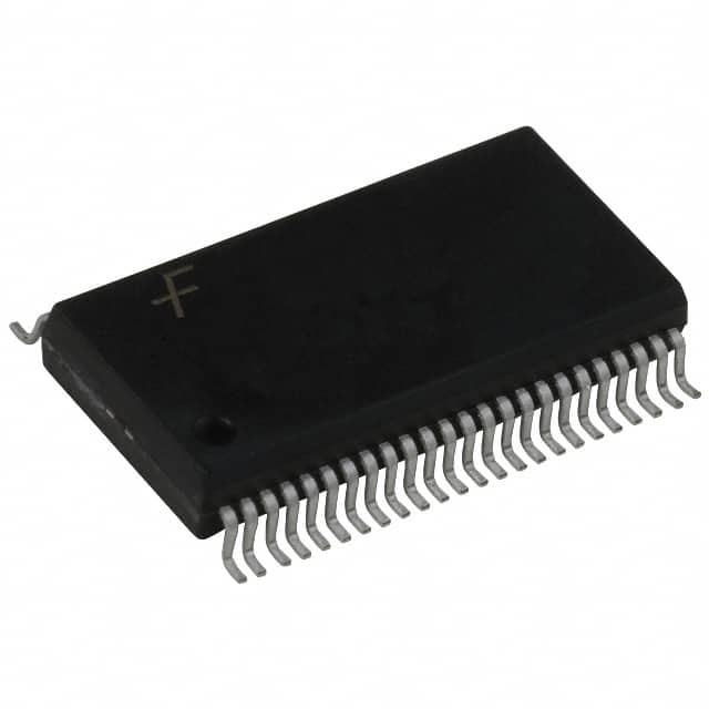
The 74ABT16374CSSC is available in a small-outline integrated circuit (SOIC) package. Each package contains one unit of the IC.
Specifications
- Number of Flip-Flops: 16
- Logic Family: ABT
- Logic Type: D-Type Transparent Latch
- Clock Trigger: Positive Edge
- Data Input Type: Standard
- Output Type: Tri-State
- Operating Voltage Range: 2.0V - 5.5V
- Operating Temperature Range: -40°C to +85°C
Pin Configuration
The detailed pin configuration of the 74ABT16374CSSC is as follows:
- Pin 1: Data Input (D0)
- Pin 2: Data Input (D1)
- Pin 3: Data Input (D2)
- Pin 4: Data Input (D3)
- Pin 5: Data Input (D4)
- Pin 6: Data Input (D5)
- Pin 7: Data Input (D6)
- Pin 8: Data Input (D7)
- Pin 9: GND (Ground)
- Pin 10: Data Output (Q0)
- Pin 11: Data Output (Q1)
- Pin 12: Data Output (Q2)
- Pin 13: Data Output (Q3)
- Pin 14: Data Output (Q4)
- Pin 15: Data Output (Q5)
- Pin 16: Data Output (Q6)
- Pin 17: Data Output (Q7)
- Pin 18: Clock Input (CP)
- Pin 19: Output Enable (OE)
- Pin 20: VCC (Power Supply)
Functional Features
The 74ABT16374CSSC offers the following functional features: - Transparent latch operation: The IC allows data to be latched and stored when the clock input is high. - Tri-state outputs: It provides tri-state outputs, allowing multiple devices to share a common bus without interference. - Output enable control: The output enable pin enables or disables the data outputs, providing flexibility in controlling data flow.
Advantages and Disadvantages
Advantages: - High-speed operation facilitates time-critical applications. - Low power consumption ensures efficient energy usage. - Wide operating voltage range enhances compatibility. - Strong output drive capability enables efficient driving of capacitive loads. - ESD protection safeguards against static electricity damage.
Disadvantages: - Limited number of flip-flops (16) may not be sufficient for certain complex applications. - Availability in only one package type (SOIC) may limit compatibility with specific circuit designs.
Working Principles
The 74ABT16374CSSC operates based on the principles of sequential logic. It utilizes transparent latch operation, where data is latched and stored when the clock input transitions from low to high. The tri-state outputs allow the IC to control data flow effectively.
Application Field Plans
The 74ABT16374CSSC finds extensive application in various digital systems, including but not limited to: - Microprocessors and microcontrollers - Memory modules and storage devices - Communication devices and networking equipment - Industrial automation systems - Automotive electronics
Alternative Models
For those seeking alternative models with similar functionality, the following options are available: - 74HC16374: This IC offers comparable features and pin configuration but operates at a different voltage range (2.0V - 6.0V). - SN74LV16374: This IC is another alternative with similar characteristics, but
قم بإدراج 10 أسئلة وإجابات شائعة تتعلق بتطبيق 74ABT16374CSSC في الحلول التقنية
Sure! Here are 10 common questions and answers related to the application of 74ABT16374CSSC:
Q: What is the 74ABT16374CSSC? A: The 74ABT16374CSSC is a 16-bit D-type flip-flop with 3-state outputs, commonly used in digital circuits.
Q: What is the purpose of the 74ABT16374CSSC? A: The purpose of this IC is to store and transfer data in digital systems, providing sequential logic functionality.
Q: How many flip-flops are there in the 74ABT16374CSSC? A: The 74ABT16374CSSC contains 16 individual flip-flops, each capable of storing one bit of data.
Q: What is the maximum clock frequency supported by the 74ABT16374CSSC? A: The maximum clock frequency supported by this IC is typically specified in its datasheet, which can vary depending on the manufacturer.
Q: Can I use the 74ABT16374CSSC for level shifting applications? A: Yes, the 74ABT16374CSSC can be used for level shifting as it supports both TTL and CMOS voltage levels.
Q: How do I connect the inputs and outputs of the 74ABT16374CSSC? A: The inputs and outputs of this IC should be connected according to the pinout diagram provided in its datasheet.
Q: Can I cascade multiple 74ABT16374CSSC ICs together? A: Yes, you can cascade multiple 74ABT16374CSSC ICs to increase the number of bits stored or transferred.
Q: What is the power supply voltage range for the 74ABT16374CSSC? A: The power supply voltage range for this IC typically ranges from 4.5V to 5.5V, but it's important to refer to the datasheet for precise specifications.
Q: Does the 74ABT16374CSSC have any built-in protection features? A: Yes, this IC usually includes built-in protection against electrostatic discharge (ESD) and excessive current.
Q: Are there any specific timing considerations when using the 74ABT16374CSSC? A: Yes, timing considerations such as setup time, hold time, and propagation delay should be taken into account when designing with this IC. Refer to the datasheet for detailed timing specifications.
Please note that the answers provided here are general and may vary depending on the specific manufacturer's datasheet and application requirements.