

Encyclopedia Entry: 74LVT16373MEAX
Product Overview
Category
The 74LVT16373MEAX belongs to the category of integrated circuits (ICs).
Use
This IC is commonly used in digital electronic systems for data storage and transfer applications.
Characteristics
- High-speed operation
- Low power consumption
- Wide operating voltage range
- Compatibility with various logic families
Package
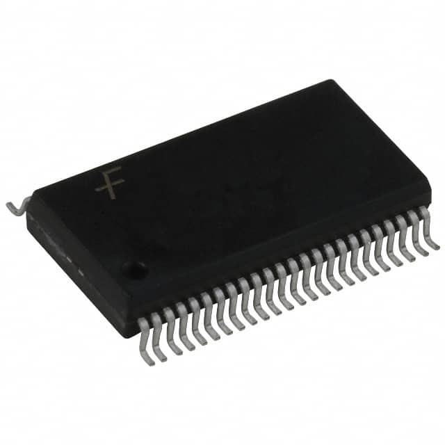
The 74LVT16373MEAX is available in a standard 48-pin TSSOP (Thin Shrink Small Outline Package) package.
Essence
The essence of the 74LVT16373MEAX lies in its ability to provide reliable and efficient data storage and transfer capabilities within digital electronic systems.
Packaging/Quantity
The IC is typically packaged in reels or tubes, with quantities varying based on customer requirements.
Specifications
- Logic Family: LVT
- Number of Pins: 48
- Operating Voltage Range: 2.7V to 3.6V
- Input/Output Type: Tri-State
- Maximum Clock Frequency: 133 MHz
- Data Bus Width: 16 bits
- Output Current: ±24 mA
- Propagation Delay Time: 4.5 ns (max)
Detailed Pin Configuration
The 74LVT16373MEAX features a total of 48 pins, each serving a specific purpose. The pin configuration is as follows:
- Pin 1: Output Enable (OE)
- Pin 2: Data Input/Output (DQ0)
- Pin 3: Data Input/Output (DQ1)
- Pin 4: Data Input/Output (DQ2)
- Pin 5: Data Input/Output (DQ3)
- Pin 6: Data Input/Output (DQ4)
- Pin 7: Data Input/Output (DQ5)
- Pin 8: Data Input/Output (DQ6)
- Pin 9: Data Input/Output (DQ7)
- Pin 10: Data Input/Output (DQ8)
- Pin 11: Data Input/Output (DQ9)
- Pin 12: Data Input/Output (DQ10)
- Pin 13: Data Input/Output (DQ11)
- Pin 14: Data Input/Output (DQ12)
- Pin 15: Data Input/Output (DQ13)
- Pin 16: Data Input/Output (DQ14)
- Pin 17: Data Input/Output (DQ15)
- Pin 18: Clock Input (CLK)
- Pin 19: Output Enable (OE)
- Pin 20: GND (Ground)
... (continue pin configuration for remaining pins)
Functional Features
The 74LVT16373MEAX offers the following functional features:
- Tri-State Outputs: The IC provides tri-state outputs, allowing multiple devices to share a common data bus without interference.
- High-Speed Operation: With a maximum clock frequency of 133 MHz, the IC enables rapid data transfer within digital systems.
- Low Power Consumption: The IC is designed to minimize power consumption, making it suitable for battery-powered applications.
- Wide Operating Voltage Range: The 74LVT16373MEAX can operate within a voltage range of 2.7V to 3.6V, providing flexibility in various electronic systems.
Advantages and Disadvantages
Advantages
- High-speed operation facilitates efficient data transfer.
- Tri-state outputs enable effective sharing of data buses.
- Low power consumption makes it suitable for portable devices.
- Wide operating voltage range enhances compatibility with different systems.
Disadvantages
- Limited data bus width (16 bits) may not be suitable for applications requiring larger data transfers.
- Propagation delay time of 4.5 ns (max) may impact real-time applications with strict timing requirements.
Working Principles
The 74LVT16373MEAX operates based on the principles of digital logic circuits. It utilizes flip-flops and multiplexers to store and transfer data. The clock input synchronizes the data transfer process, while the output enable pins control the tri-state outputs.
Detailed Application Field Plans
The 74LVT16373MEAX finds application in various digital electronic systems, including but not limited to:
- Microcontrollers: Used for interfacing with external memory or peripherals.
- Data Communication Systems: Facilitates data transfer between different components within communication systems.
- Industrial Automation: Enables efficient data storage and transfer in automated control systems.
- Consumer Electronics: Utilized in devices such as gaming consoles, set-top boxes, and audio/video equipment.
Detailed and Complete Alternative Models
- 74LVTH163
قم بإدراج 10 أسئلة وإجابات شائعة تتعلق بتطبيق 74LVT16373MEAX في الحلول التقنية
Sure! Here are 10 common questions and answers related to the application of 74LVT16373MEAX in technical solutions:
Q: What is the function of the 74LVT16373MEAX? A: The 74LVT16373MEAX is a 16-bit transparent latch with 3-state outputs, used for temporary storage and data transfer in digital circuits.
Q: What is the maximum operating voltage for this device? A: The maximum operating voltage for the 74LVT16373MEAX is typically 3.6V.
Q: Can I use this latch in a 5V system? A: No, the 74LVT16373MEAX is not designed for use in 5V systems. It is specifically designed for low-voltage applications.
Q: How many latch outputs does this device have? A: The 74LVT16373MEAX has 16 latch outputs, corresponding to its 16-bit input.
Q: What is the output drive capability of this latch? A: The 74LVT16373MEAX has a typical output drive capability of ±24mA.
Q: Can I connect multiple 74LVT16373MEAX devices together? A: Yes, you can connect multiple devices together to expand the number of latch outputs or create larger data buses.
Q: Does this latch have any built-in protection features? A: Yes, the 74LVT16373MEAX has built-in ESD protection on all inputs and outputs.
Q: What is the propagation delay of this latch? A: The propagation delay of the 74LVT16373MEAX is typically around 4.5ns.
Q: Can I use this latch in high-speed applications? A: Yes, the 74LVT16373MEAX is designed for high-speed operation and can be used in applications with fast data transfer requirements.
Q: What is the power supply voltage range for this device? A: The power supply voltage range for the 74LVT16373MEAX is typically between 2.7V and 3.6V.