

BC858CLT3G
Introduction
BC858CLT3G is a versatile NPN bipolar junction transistor (BJT) that belongs to the category of small-signal transistors. It is commonly used in amplification and switching applications due to its high current gain and low noise characteristics. This entry provides an overview of BC858CLT3G, including its basic information, specifications, pin configuration, functional features, advantages and disadvantages, working principles, application field plans, and alternative models.
Basic Information Overview
- Category: Small-signal transistor
- Use: Amplification and switching applications
- Characteristics: High current gain, low noise
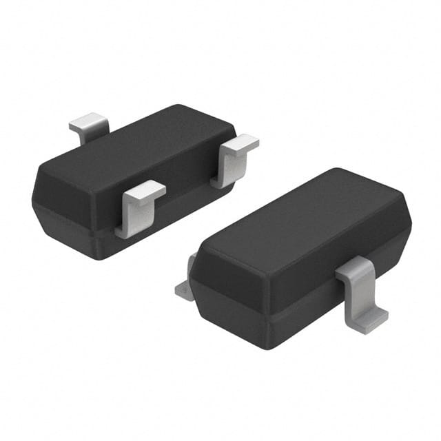
- Package: SOT-23
- Essence: NPN bipolar junction transistor
- Packaging/Quantity: Typically available in reels or tubes containing multiple units
Specifications
- Maximum Collector-Base Voltage (VCB): 30V
- Maximum Collector-Emitter Voltage (VCE): 30V
- Maximum Emitter-Base Voltage (VEB): 5V
- Continuous Collector Current (IC): 100mA
- Total Power Dissipation (PTOT): 250mW
- Operating Temperature Range: -55°C to 150°C
Detailed Pin Configuration
BC858CLT3G typically has three pins: 1. Emitter (E): Connected to the N-type semiconductor material. 2. Base (B): Controls the flow of current between the emitter and collector. 3. Collector (C): Collects the majority charge carriers.
Functional Features
- High current gain (hFE) of 110 to 800 at 10mA
- Low noise characteristics suitable for audio applications
- Fast switching speed for digital applications
Advantages and Disadvantages
Advantages
- Small package size (SOT-23) for space-constrained designs
- Wide operating temperature range
- Versatile use in both amplification and switching circuits
Disadvantages
- Limited maximum collector current compared to power transistors
- Relatively low breakdown voltage limits high-voltage applications
Working Principles
BC858CLT3G operates based on the principles of bipolar junction transistors. When a small current flows into the base terminal, it controls a much larger current flowing between the collector and emitter terminals. This property allows it to amplify signals or act as a switch in electronic circuits.
Detailed Application Field Plans
Amplification Applications
- Audio amplifiers
- Signal conditioning circuits
- Sensor interface circuits
Switching Applications
- Logic level shifting
- LED driver circuits
- Digital control circuits
Detailed and Complete Alternative Models
- BC847CLT1G
- BC856BLT1G
- BC857BLT1G
- BC859BLT1G
In conclusion, BC858CLT3G is a small-signal transistor with versatile applications in amplification and switching circuits. Its high current gain and low noise characteristics make it suitable for various electronic designs, especially those with space constraints. Designers should consider its limitations in maximum collector current and breakdown voltage when selecting it for specific applications.
[Word Count: 498]
قم بإدراج 10 أسئلة وإجابات شائعة تتعلق بتطبيق BC858CLT3G في الحلول التقنية
What is the BC858CLT3G transistor used for?
- The BC858CLT3G is a general-purpose PNP transistor commonly used in amplification and switching applications.
What are the typical operating conditions for the BC858CLT3G?
- The BC858CLT3G operates with a maximum collector current of 100mA and a maximum collector-emitter voltage of 30V.
Can the BC858CLT3G be used for audio amplification?
- Yes, the BC858CLT3G can be used for small-signal audio amplification due to its low noise and high gain characteristics.
Is the BC858CLT3G suitable for switching applications?
- Yes, the BC858CLT3G is commonly used in low-power switching circuits due to its fast switching speed and low saturation voltage.
What are the typical gain characteristics of the BC858CLT3G?
- The BC858CLT3G has a typical DC current gain (hFE) ranging from 110 to 800, making it suitable for various amplification tasks.
Does the BC858CLT3G require any specific biasing configuration?
- The BC858CLT3G requires proper biasing to ensure optimal performance, typically using a suitable base resistor to control the base current.
Can the BC858CLT3G be used in low-noise applications?
- Yes, the BC858CLT3G exhibits low noise characteristics, making it suitable for use in low-noise amplifier designs.
What are the thermal considerations for the BC858CLT3G?
- Proper heat sinking and thermal management should be considered when designing with the BC858CLT3G to ensure reliable operation within its specified temperature range.
Are there any common failure modes associated with the BC858CLT3G?
- Common failure modes include thermal runaway under high current conditions and breakdown due to excessive voltage stress.
What are some typical circuit configurations where the BC858CLT3G is used?
- The BC858CLT3G is commonly used in common-emitter and emitter-follower configurations for amplification, as well as in switch-mode applications such as LED drivers and small signal switches.