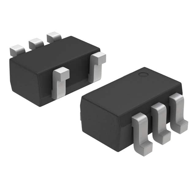
MC74VHC1G125DFT1G
Product Overview
- Category: Integrated Circuit
- Use: Logic Gate Buffer/Driver
- Characteristics: High-Speed, Low-Power, Single Gate
- Package: SOT-353 (SC-88A)
- Essence: Buffer/Driver for Digital Signals
- Packaging/Quantity: Tape and Reel, 3000 units per reel
Specifications
- Supply Voltage: 2.0V to 5.5V
- Input Voltage: 0V to VCC
- Output Voltage: 0V to VCC
- Operating Temperature: -40°C to +85°C
- Propagation Delay: 3.4ns (typical) at 5V
- Output Drive Capability: ±8mA at 5V
Pin Configuration
The MC74VHC1G125DFT1G has a total of 5 pins:
- GND: Ground reference voltage.
- A: Input pin for the digital signal.
- OE: Output Enable pin.
- Y: Output pin for the buffered signal.
- VCC: Positive supply voltage.
Functional Features
- Provides buffering and driving capability for digital signals.
- Supports high-speed operation with low power consumption.
- Offers a single gate solution for compact designs.
- Enables easy integration into various digital systems.
Advantages
- High-speed operation allows for efficient signal processing.
- Low-power consumption helps in reducing overall energy usage.
- Single gate design saves space and simplifies circuit layout.
- Wide supply voltage range enhances compatibility with different systems.
Disadvantages
- Limited output drive capability may restrict use in certain applications.
- Operating temperature range may not be suitable for extreme environments.
- Availability of alternative models with additional features may be limited.
Working Principles
The MC74VHC1G125DFT1G is a logic gate buffer/driver that amplifies and shapes digital signals. It operates by receiving an input signal at pin A, which is then buffered and amplified to provide a clean output signal at pin Y. The OE pin controls the output enable function, allowing the user to enable or disable the output as needed. The device operates within a specified supply voltage range and converts the input signal into a corresponding output signal with minimal delay.
Detailed Application Field Plans
The MC74VHC1G125DFT1G finds applications in various fields where buffering and driving of digital signals are required. Some potential application areas include:
- Communication Systems: Used for signal conditioning and level shifting in data transmission systems.
- Industrial Automation: Enables interfacing between different digital components in control systems.
- Consumer Electronics: Provides signal buffering in devices such as smartphones, tablets, and gaming consoles.
- Automotive Electronics: Used for signal amplification and shaping in automotive control units and infotainment systems.
- Medical Devices: Enables signal conditioning and amplification in medical equipment and monitoring systems.
Detailed Alternative Models
While the MC74VHC1G125DFT1G offers a compact and efficient solution for buffering and driving digital signals, there are alternative models available in the market. Some notable alternatives include:
- SN74LVC1G125DBVR: Similar functionality with enhanced output drive capability.
- NC7SZ125P5X: Ultra-small package size with comparable performance characteristics.
- 74AUP1G125GW: Low-power variant with extended operating temperature range.
These alternative models provide users with options based on specific requirements and design constraints.
In conclusion, the MC74VHC1G125DFT1G is a high-speed, low-power logic gate buffer/driver that offers efficient signal buffering and driving capabilities. Its compact design and wide supply voltage range make it suitable for various digital systems. However, users should consider alternative models based on specific application needs and additional features required.
قم بإدراج 10 أسئلة وإجابات شائعة تتعلق بتطبيق MC74VHC1G125DFT1G في الحلول التقنية
Sure! Here are 10 common questions and answers related to the application of MC74VHC1G125DFT1G in technical solutions:
1. What is MC74VHC1G125DFT1G? MC74VHC1G125DFT1G is a single bus buffer gate with 3-state output, designed for use in high-performance digital systems.
2. What is the operating voltage range of MC74VHC1G125DFT1G? The operating voltage range of MC74VHC1G125DFT1G is from 2.0V to 5.5V.
3. What is the maximum output current of MC74VHC1G125DFT1G? The maximum output current of MC74VHC1G125DFT1G is 8mA.
4. Can MC74VHC1G125DFT1G be used as a level shifter? Yes, MC74VHC1G125DFT1G can be used as a level shifter to convert signals between different voltage levels.
5. What is the propagation delay of MC74VHC1G125DFT1G? The propagation delay of MC74VHC1G125DFT1G is typically 4.3ns.
6. Is MC74VHC1G125DFT1G compatible with other logic families? Yes, MC74VHC1G125DFT1G is compatible with both CMOS and TTL logic families.
7. Can MC74VHC1G125DFT1G be used in battery-powered applications? Yes, MC74VHC1G125DFT1G can be used in battery-powered applications due to its low power consumption.
8. Does MC74VHC1G125DFT1G have built-in ESD protection? Yes, MC74VHC1G125DFT1G has built-in ESD protection to ensure reliability in harsh environments.
9. What is the package type of MC74VHC1G125DFT1G? MC74VHC1G125DFT1G is available in a small SOT-353 package.
10. Can MC74VHC1G125DFT1G be used in automotive applications? Yes, MC74VHC1G125DFT1G is qualified for automotive applications and meets the AEC-Q100 standard.
Please note that these answers are general and may vary depending on the specific datasheet and application requirements.


