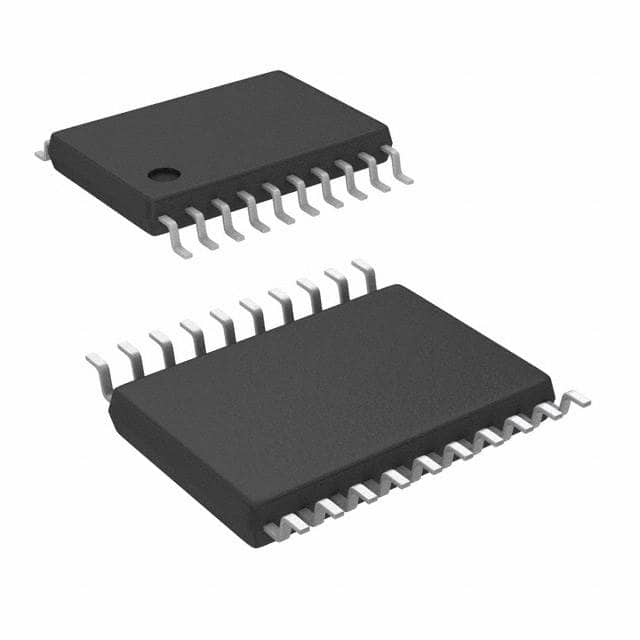
MC74VHCT244ADTG
Overview
- Category: Integrated Circuit (IC)
- Use: Buffer/Line Driver
- Characteristics: High-Speed, Low-Power, TTL-Compatible
- Package: TSSOP-20
- Essence: Voltage-Level Shifter
- Packaging/Quantity: Tape and Reel, 2500 units per reel
Specifications
- Supply Voltage Range: 2.0V to 5.5V
- Input Voltage Range: 0V to VCC
- Output Voltage Range: 0V to VCC
- Maximum Operating Frequency: 125 MHz
- Propagation Delay Time: 4.3 ns (typical)
- Output Drive Capability: ±24 mA
Pin Configuration
The MC74VHCT244ADTG has a total of 20 pins. The pin configuration is as follows:
- A1
- Y1
- A2
- GND
- Y2
- A3
- A4
- Y3
- A5
- VCC
- Y4
- A6
- A7
- Y5
- A8
- GND
- Y6
- A9
- Y7
- Y8
Functional Features
- High-Speed Operation: The MC74VHCT244ADTG is designed for high-speed data transmission, making it suitable for applications requiring fast signal propagation.
- Low Power Consumption: This IC operates at low power levels, reducing energy consumption and extending battery life in portable devices.
- TTL-Compatible Inputs: The inputs are compatible with TTL logic levels, allowing seamless integration with existing TTL-based systems.
- Wide Supply Voltage Range: The IC can operate within a wide supply voltage range, providing flexibility in various applications.
Advantages and Disadvantages
Advantages: - High-speed operation enables efficient data transmission. - Low power consumption extends battery life. - TTL compatibility allows easy integration with existing systems. - Wide supply voltage range provides flexibility.
Disadvantages: - Limited output drive capability may not be suitable for high-current applications. - Propagation delay time may affect timing-sensitive applications.
Working Principles
The MC74VHCT244ADTG is a voltage-level shifter that converts signals from one voltage level to another. It consists of eight bidirectional buffers, each capable of shifting the logic levels of input signals. The IC operates by receiving input signals on the A1-A9 pins and providing corresponding output signals on the Y1-Y8 pins. The voltage levels of the input and output signals are determined by the supply voltage applied to the VCC pin.
Detailed Application Field Plans
The MC74VHCT244ADTG can be used in various applications, including:
- Data Communication: It can be used as a buffer/line driver in data communication systems to ensure reliable signal transmission between different voltage domains.
- Microcontroller Interfacing: The IC can be employed to interface microcontrollers operating at different voltage levels, enabling seamless communication between them.
- Level Shifting: It can be utilized to shift voltage levels in mixed-signal circuits, allowing compatibility between devices operating at different logic levels.
- Signal Conditioning: The MC74VHCT244ADTG can be used to condition signals in analog-to-digital converters (ADCs) or digital-to-analog converters (DACs), ensuring accurate conversion.
Detailed and Complete Alternative Models
- SN74LVC244A: This IC offers similar functionality and characteristics to the MC74VHCT244ADTG, but operates at a lower supply voltage range of 1.65V to 3.6V.
- 74HC244: This IC is a TTL-compatible octal buffer/line driver with similar specifications and pin configuration to the MC74VHCT244ADTG, but operates at a higher supply voltage range of 2.0V to 6.0V.
(Note: The above alternative models are provided for reference and may have slight variations in characteristics and package options. It is recommended to refer to the respective datasheets for detailed information.)
In conclusion, the MC74VHCT244ADTG is a high-speed, low-power buffer/line driver IC that provides voltage-level shifting capabilities. Its wide supply voltage range, TTL compatibility, and compact TSSOP-20 package make it suitable for various applications in data communication, microcontroller interfacing, level shifting, and signal conditioning. Alternative models such as the SN74LVC244A and 74HC244 offer similar functionality with slight variations in specifications and operating parameters.
قم بإدراج 10 أسئلة وإجابات شائعة تتعلق بتطبيق MC74VHCT244ADTG في الحلول التقنية
Sure! Here are 10 common questions and answers related to the application of MC74VHCT244ADTG in technical solutions:
Q: What is MC74VHCT244ADTG? A: MC74VHCT244ADTG is a high-speed CMOS octal buffer/line driver with 3-state outputs.
Q: What is the voltage range supported by MC74VHCT244ADTG? A: MC74VHCT244ADTG supports a voltage range from 4.5V to 5.5V.
Q: What is the maximum operating frequency of MC74VHCT244ADTG? A: The maximum operating frequency of MC74VHCT244ADTG is typically around 125 MHz.
Q: Can MC74VHCT244ADTG be used for level shifting applications? A: Yes, MC74VHCT244ADTG can be used for level shifting between different voltage domains.
Q: How many input/output pins does MC74VHCT244ADTG have? A: MC74VHCT244ADTG has 8 input pins and 8 output pins.
Q: Is MC74VHCT244ADTG compatible with TTL logic levels? A: Yes, MC74VHCT244ADTG is compatible with both TTL and CMOS logic levels.
Q: What is the maximum output current that MC74VHCT244ADTG can drive? A: MC74VHCT244ADTG can drive up to 8 mA of output current per channel.
Q: Can MC74VHCT244ADTG be used in bidirectional data transfer applications? A: No, MC74VHCT244ADTG is a unidirectional buffer and cannot be used for bidirectional data transfer.
Q: Does MC74VHCT244ADTG have built-in protection features? A: Yes, MC74VHCT244ADTG has built-in ESD protection on all inputs and outputs.
Q: What package options are available for MC74VHCT244ADTG? A: MC74VHCT244ADTG is available in various package options, such as TSSOP, SOIC, and PDIP.
Please note that these answers are general and may vary depending on the specific datasheet and manufacturer's specifications of MC74VHCT244ADTG.


