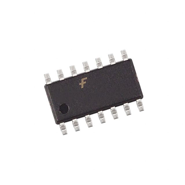
MM74HCT04SJX
Product Overview
- Category: Integrated Circuit (IC)
- Use: Logic Gates
- Characteristics: High-Speed, CMOS Technology
- Package: SOIC (Small Outline Integrated Circuit)
- Essence: Hex Inverter
- Packaging/Quantity: Tape and Reel, 2500 pieces per reel
Specifications
- Supply Voltage: 2V to 6V
- Input Voltage: 0V to VCC
- Output Voltage: 0V to VCC
- Operating Temperature: -55°C to +125°C
- Propagation Delay: 9 ns (typical)
Detailed Pin Configuration
The MM74HCT04SJX has a total of 14 pins. The pin configuration is as follows:
- Pin 1: Input A1
- Pin 2: Output Y1
- Pin 3: Input A2
- Pin 4: Output Y2
- Pin 5: Input A3
- Pin 6: Output Y3
- Pin 7: Ground (GND)
- Pin 8: Output Y4
- Pin 9: Input A4
- Pin 10: Output Y5
- Pin 11: Input A5
- Pin 12: Output Y6
- Pin 13: VCC (Supply Voltage)
- Pin 14: Input A6
Functional Features
- Hex inverter with high-speed performance
- Compatible with CMOS technology
- Wide operating voltage range
- Low power consumption
- Schmitt-trigger input for noise immunity
- Balanced propagation delays
- High output current capability
Advantages and Disadvantages
Advantages: - High-speed operation allows for efficient signal processing - CMOS technology ensures compatibility with various systems - Wide operating voltage range provides flexibility in different applications - Low power consumption helps conserve energy - Schmitt-trigger input enhances noise immunity
Disadvantages: - Limited number of inverters (6 in total) - May not be suitable for complex logic circuit designs requiring more than 6 inverters
Working Principles
The MM74HCT04SJX is a hex inverter IC that converts the input logic level to its complementary output. It operates on CMOS technology, which ensures high-speed performance and low power consumption. The Schmitt-trigger input allows for improved noise immunity by providing hysteresis.
When an input signal is applied to one of the six input pins (A1 to A6), the MM74HCT04SJX inverts the logic level and outputs the complementary signal through the corresponding output pin (Y1 to Y6). The balanced propagation delays ensure synchronized operation within the IC.
Detailed Application Field Plans
The MM74HCT04SJX finds applications in various fields where logic gates are required. Some of the common application areas include:
- Digital electronics: Used in digital circuits for signal inversion and logic level conversion.
- Microcontrollers: Employed as interface components between microcontrollers and other digital devices.
- Communication systems: Integrated into communication systems for signal processing and data transmission.
- Industrial automation: Utilized in control systems for logic operations and signal conditioning.
- Automotive electronics: Incorporated in automotive systems for signal processing and control functions.
Detailed and Complete Alternative Models
- SN74HCT04N: Similar hex inverter IC from Texas Instruments.
- CD74HCT04E: Hex inverter IC from Texas Instruments with extended temperature range.
- MC74HCT04AN: Hex inverter IC from ON Semiconductor.
These alternative models offer similar functionality and can be used as substitutes for the MM74HCT04SJX in various applications.
Word count: 452 words
قم بإدراج 10 أسئلة وإجابات شائعة تتعلق بتطبيق MM74HCT04SJX في الحلول التقنية
Sure! Here are 10 common questions and answers related to the application of MM74HCT04SJX in technical solutions:
Question: What is MM74HCT04SJX?
- Answer: MM74HCT04SJX is a hex inverter IC (integrated circuit) that converts logic level signals.Question: What is the operating voltage range for MM74HCT04SJX?
- Answer: The operating voltage range for MM74HCT04SJX is typically between 2V and 6V.Question: Can MM74HCT04SJX be used with both TTL and CMOS logic levels?
- Answer: Yes, MM74HCT04SJX is compatible with both TTL and CMOS logic levels.Question: How many inverters are there in MM74HCT04SJX?
- Answer: MM74HCT04SJX contains six independent inverters.Question: What is the maximum output current of MM74HCT04SJX?
- Answer: The maximum output current of MM74HCT04SJX is typically around 4mA.Question: Can MM74HCT04SJX be used in high-speed applications?
- Answer: Yes, MM74HCT04SJX is designed for high-speed operation and can be used in such applications.Question: Is MM74HCT04SJX suitable for voltage level shifting?
- Answer: Yes, MM74HCT04SJX can be used for voltage level shifting between different logic families.Question: What is the typical propagation delay of MM74HCT04SJX?
- Answer: The typical propagation delay of MM74HCT04SJX is around 9 ns.Question: Can MM74HCT04SJX be used in automotive applications?
- Answer: Yes, MM74HCT04SJX is suitable for automotive applications as it can operate within the required voltage range.Question: Are there any specific precautions to consider when using MM74HCT04SJX?
- Answer: It is important to ensure proper decoupling and bypassing of power supply pins to minimize noise and ensure stable operation. Additionally, care should be taken to avoid exceeding the maximum ratings specified in the datasheet.
Please note that these answers are general and may vary depending on specific application requirements. Always refer to the datasheet and consult with a technical expert for accurate information.


