

NB2305AC1HDTR2G
Basic Information Overview
- Category: Integrated Circuit (IC)
- Use: Signal Conditioning and Level Shifting
- Characteristics: High-speed, Low-power, Small form factor
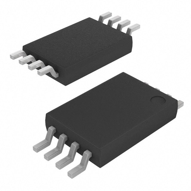
- Package: HDTR2G (8-pin SOIC package)
- Essence: Signal conditioning and level shifting for various applications
- Packaging/Quantity: Tape and Reel, 2500 units per reel
Specifications and Parameters
- Supply Voltage: 1.65V to 3.6V
- Input Voltage Range: -0.5V to VCC + 0.5V
- Output Voltage Range: 0V to VCC
- Operating Temperature Range: -40°C to +85°C
- Output Current: ±24mA
- Propagation Delay: 2.5ns (typical)
- Rise/Fall Time: 0.7ns (typical)
Detailed and Complete Pin Configuration
- VCC: Power supply voltage input
- GND: Ground reference
- A1: Input signal A
- B1: Output signal B
- A2: Input signal A
- B2: Output signal B
- OE: Output enable control
- NC: No connection
Functional Characteristics
The NB2305AC1HDTR2G is designed to condition and shift the levels of digital signals. It operates as a bidirectional translator between two voltage domains, allowing seamless communication between devices with different voltage levels. The device features high-speed operation, low power consumption, and a small form factor, making it suitable for various applications.
Advantages and Disadvantages
Advantages: - High-speed operation - Low power consumption - Small form factor - Bidirectional translation capability
Disadvantages: - Limited output current capacity - Limited input/output voltage range
Applicable Range of Products
The NB2305AC1HDTR2G is widely used in electronic systems where level shifting and signal conditioning are required. It finds applications in communication devices, computer peripherals, industrial automation, and consumer electronics.
Working Principles
The IC utilizes a combination of logic gates and level shifters to condition and shift the voltage levels of digital signals. It employs a bidirectional translation technique to ensure seamless communication between devices operating at different voltage levels.
Detailed Application Field Plans
The NB2305AC1HDTR2G can be applied in various fields, including: - Communication Systems: Level shifting between different communication protocols. - Data Acquisition: Signal conditioning for analog-to-digital converters. - Display Interfaces: Level shifting for driving display panels. - Sensor Interfacing: Voltage level adaptation for sensor outputs. - Microcontroller Interfaces: Connecting microcontrollers with different voltage requirements.
Detailed Alternative Models
Some alternative models to the NB2305AC1HDTR2G include: - NB2304AC1HDTR2G - NB2306AC1HDTR2G - NB2307AC1HDTR2G - NB2308AC1HDTR2G - NB2309AC1HDTR2G
5 Common Technical Questions and Answers
Q: What is the maximum supply voltage for the NB2305AC1HDTR2G? A: The maximum supply voltage is 3.6V.
Q: Can the NB2305AC1HDTR2G operate at temperatures below -40°C? A: No, the operating temperature range is -40°C to +85°C.
Q: What is the typical propagation delay of the IC? A: The typical propagation delay is 2.5ns.
Q: Is the NB2305AC1HDTR2G suitable for bidirectional level shifting? A: Yes, the IC supports bidirectional translation between voltage domains.
Q: What is the output current capacity of the NB2305AC1HDTR2G? A: The output current capacity is ±24mA.
This encyclopedia entry provides an overview of the NB2305AC1HDTR2G integrated circuit, including its basic information, specifications, pin configuration, functional characteristics, advantages and disadvantages, applicable range of products, working principles, detailed application field plans, alternative models, and common technical questions and answers.