

NB4N441MNR2G
Product Overview
- Category: Integrated Circuit
- Use: Signal Conditioning and Clock Generation
- Characteristics: High-speed, Low-power, Differential Receiver
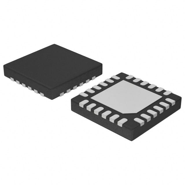
- Package: 32-pin QFN (Quad Flat No-Lead)
- Essence: Signal conditioning and clock generation for high-speed data transmission
- Packaging/Quantity: Tape and Reel, 2500 units per reel
Specifications
- Supply Voltage: 3.3V
- Operating Temperature Range: -40°C to +85°C
- Input Frequency Range: DC to 2.5 GHz
- Differential Input Voltage Range: ±1V
- Output Voltage Swing: 400mV to 1.6V
- Propagation Delay: 200ps
- Power Dissipation: 150mW
Detailed Pin Configuration
The NB4N441MNR2G has a total of 32 pins arranged as follows:
- VDDA
- VSSA
- CLKIN_P
- CLKIN_N
- CLKOUT_P
- CLKOUT_N
- VDDO
- VSSO
- OE#
- SEL
- NC
- NC
- NC
- NC
- NC
- NC
- NC
- NC
- NC
- NC
- NC
- NC
- NC
- NC
- NC
- NC
- NC
- NC
- NC
- NC
- NC
- NC
Functional Features
- High-speed differential receiver with low propagation delay
- Supports wide input frequency range for signal conditioning
- Provides clock generation capability for synchronized data transmission
- Low-power consumption for energy-efficient operation
- Differential input voltage range allows for versatile signal compatibility
Advantages and Disadvantages
Advantages
- High-speed operation enables efficient data transmission
- Low-power design reduces energy consumption
- Wide input frequency range accommodates various signal types
- Compact package size saves board space
- Differential receiver enhances noise immunity
Disadvantages
- Limited pin configuration options may restrict certain applications
- Propagation delay may affect real-time systems with strict timing requirements
Working Principles
The NB4N441MNR2G is designed to condition and generate clock signals for high-speed data transmission. It operates by receiving differential input signals through CLKINP and CLKINN pins, which are then processed and amplified. The device also generates a synchronized clock output through CLKOUTP and CLKOUTN pins. This clock signal can be used to drive other components in the system.
Detailed Application Field Plans
The NB4N441MNR2G finds application in various fields, including:
- Telecommunications: Used in high-speed data communication systems, such as fiber optic networks.
- Networking: Enables clock synchronization in Ethernet switches and routers.
- Test and Measurement: Provides signal conditioning and clock generation capabilities in test equipment.
- Industrial Automation: Supports data transmission in industrial control systems.
- Automotive: Used in automotive electronics for signal conditioning and clock generation.
Detailed and Complete Alternative Models
- NB4N11S: Single-ended to differential converter IC.
- NB4N111K: Differential receiver with selectable input threshold levels.
- NB4N121K: Differential receiver with integrated termination resistors.
- NB4N311K: Differential receiver with adjustable output swing levels.
- NB4N441K: Higher-speed version of NB4N441MNR2G with lower propagation delay.
(Note: The above alternative models are provided for reference and may have different specifications and pin configurations.)
Word count: 439 words
قم بإدراج 10 أسئلة وإجابات شائعة تتعلق بتطبيق NB4N441MNR2G في الحلول التقنية
Sure! Here are 10 common questions and answers related to the application of NB4N441MNR2G in technical solutions:
Q: What is NB4N441MNR2G? A: NB4N441MNR2G is a high-speed differential receiver designed for use in various technical applications.
Q: What is the maximum data rate supported by NB4N441MNR2G? A: NB4N441MNR2G supports a maximum data rate of up to 2.5 Gbps.
Q: What is the operating voltage range of NB4N441MNR2G? A: The operating voltage range of NB4N441MNR2G is typically between 3.0V and 3.6V.
Q: Can NB4N441MNR2G be used in low-power applications? A: Yes, NB4N441MNR2G has a low power consumption and can be used in low-power applications.
Q: What is the input common-mode voltage range of NB4N441MNR2G? A: The input common-mode voltage range of NB4N441MNR2G is typically between -0.5V and VCC+0.5V.
Q: Does NB4N441MNR2G have built-in ESD protection? A: Yes, NB4N441MNR2G has built-in ESD protection to ensure robustness against electrostatic discharge.
Q: Can NB4N441MNR2G be used in high-speed communication systems? A: Yes, NB4N441MNR2G is specifically designed for high-speed communication systems and can be used in such applications.
Q: What is the output voltage swing of NB4N441MNR2G? A: The output voltage swing of NB4N441MNR2G is typically between 400mV and VCC-400mV.
Q: Is NB4N441MNR2G compatible with different logic families? A: Yes, NB4N441MNR2G is compatible with various logic families such as LVPECL, CML, and LVDS.
Q: Can NB4N441MNR2G be used in automotive applications? A: Yes, NB4N441MNR2G is qualified for automotive applications and can be used in automotive systems.
Please note that these answers are general and may vary depending on the specific datasheet and application requirements.