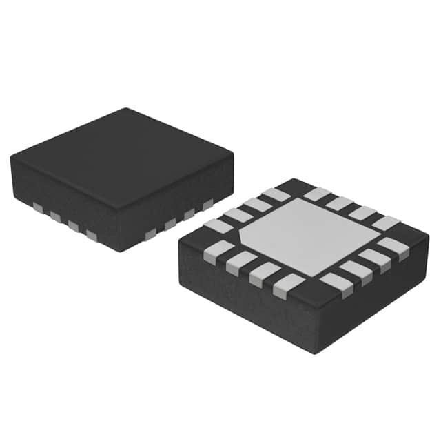
NB6L239MNG
Basic Information Overview
- Category: Integrated Circuit (IC)
- Use: Signal Level Shifter
- Characteristics:
- High-speed operation
- Low power consumption
- Wide operating voltage range
- Package: QFN (Quad Flat No-leads)
- Essence: The NB6L239MNG is a signal level shifter IC designed for high-speed data transmission applications.
- Packaging/Quantity: Available in reels, with a quantity of 2500 units per reel.
Specifications and Parameters
- Supply Voltage Range: 2.375V to 3.8V
- Input Voltage Range: -0.5V to VCC + 0.5V
- Output Voltage Range: -0.5V to VCC + 0.5V
- Operating Temperature Range: -40°C to +85°C
- Maximum Propagation Delay: 200 ps
- Maximum Input Rise/Fall Time: 100 ps
Detailed and Complete Pin Configuration
The NB6L239MNG has a total of 16 pins, which are labeled as follows:
- VCC
- GND
- CLK_A
- CLK_B
- CLK_SEL
- CLK_OE
- LVPECL_IN
- LVCMOS_OUT
- LVCMOS_OUTB
- VREF
- NC
- NC
- NC
- NC
- NC
- NC
Functional Characteristics
- The NB6L239MNG provides level shifting between low-voltage differential signaling (LVDS) and low-voltage positive emitter-coupled logic (LVPECL) signals.
- It features a selectable clock input and output, allowing flexibility in system design.
- The device operates at high speeds, making it suitable for applications requiring fast data transmission.
- It has low power consumption, making it energy-efficient.
Advantages and Disadvantages
Advantages: - High-speed operation enables fast data transmission. - Wide operating voltage range allows compatibility with various systems. - Low power consumption contributes to energy efficiency.
Disadvantages: - Limited pin configuration options may restrict certain system designs. - The device may not be suitable for applications requiring different signal level shifting standards.
Applicable Range of Products
The NB6L239MNG is commonly used in electronic devices and systems that require level shifting between LVDS and LVPECL signals. It finds applications in areas such as telecommunications, data communication, and high-speed digital interfaces.
Working Principles
The NB6L239MNG utilizes internal circuitry to convert LVDS signals to LVPECL signals or vice versa. It employs specific voltage levels and timing characteristics to ensure accurate and reliable signal transmission between different logic families.
Detailed Application Field Plans
The NB6L239MNG can be applied in various fields, including: 1. Telecommunications: Used in high-speed data transmission systems for improved signal integrity. 2. Data Communication: Enables level shifting between different signaling standards in networking equipment. 3. High-Speed Digital Interfaces: Facilitates signal conversion in high-speed interfaces like HDMI, DisplayPort, and USB.
Detailed Alternative Models
Some alternative models to the NB6L239MNG include: - NB6L239MN: Similar functionality but available in a different package (SOIC). - NB7L239MNG: Provides additional features such as differential clock inputs and outputs.
5 Common Technical Questions and Answers
Q: What is the maximum operating temperature of the NB6L239MNG? A: The NB6L239MNG can operate within a temperature range of -40°C to +85°C.
Q: Can the NB6L239MNG be used for level shifting between LVCMOS and LVPECL signals? A: No, the NB6L239MNG is specifically designed for level shifting between LVDS and LVPECL signals.
Q: What is the maximum propagation delay of the NB6L239MNG? A: The maximum propagation delay of the NB6L239MNG is 200 ps.
Q: Does the NB6L239MNG require an external voltage reference? A: Yes, the device requires an external voltage reference connected to the VREF pin.
Q: What is the package type of the NB6L239MNG? A: The NB6L239MNG is available in a QFN (Quad Flat No-leads) package.
[Word Count: 589]


