

NC7SV17L6X
Product Overview
- Category: Integrated Circuit (IC)
- Use: Logic Gate
- Characteristics: Low Voltage, Single Supply, Schmitt Trigger
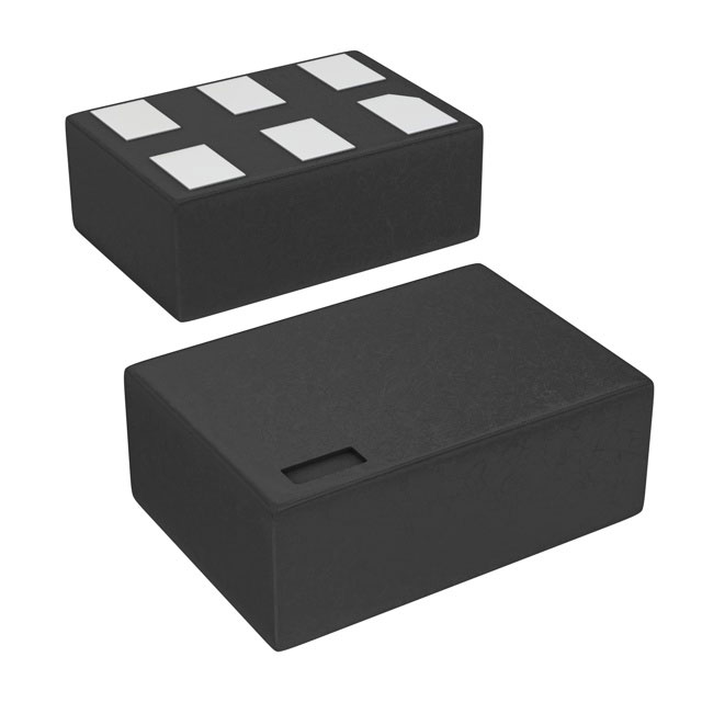
- Package: SOT-23-6
- Essence: Hex Schmitt Trigger Inverter
- Packaging/Quantity: Tape and Reel, 3000 units per reel
Specifications
- Supply Voltage Range: 1.65V to 5.5V
- Input Voltage Range: -0.5V to VCC + 0.5V
- Output Voltage Range: GND to VCC
- Operating Temperature Range: -40°C to +85°C
- Propagation Delay: 3.5 ns (typical)
- Quiescent Current: 10 µA (maximum)
Detailed Pin Configuration
The NC7SV17L6X is a hex Schmitt trigger inverter with a SOT-23-6 package. The pin configuration is as follows:
____
   A1 -|    |- VCC
   A2 -|    |- B1
   A3 -|    |- B2
  GND -|    |- C1
   A4 -|    |- C2
   A5 -|    |- D1
   A6 -|____|- D2
Functional Features
- Hex Schmitt trigger inverters provide high noise immunity and hysteresis for improved signal integrity.
- Low voltage operation allows for compatibility with various battery-powered devices.
- Single supply design simplifies circuitry and reduces component count.
- Schmitt trigger input ensures clean switching even in the presence of noisy signals.
- Fast propagation delay enables high-speed data transmission.
Advantages and Disadvantages
Advantages: - High noise immunity and hysteresis improve signal integrity. - Low voltage operation allows for compatibility with a wide range of devices. - Single supply design simplifies circuitry and reduces cost. - Schmitt trigger input ensures clean switching even in noisy environments. - Fast propagation delay enables high-speed data transmission.
Disadvantages: - Limited to hex Schmitt trigger inverter functionality. - Not suitable for applications requiring more complex logic functions.
Working Principles
The NC7SV17L6X operates as a hex Schmitt trigger inverter. It takes an input signal, applies hysteresis through the Schmitt trigger mechanism, and produces an inverted output signal. The Schmitt trigger ensures clean switching by providing two threshold voltage levels, one for rising and another for falling edges. This helps reject noise and provides improved noise immunity.
Detailed Application Field Plans
The NC7SV17L6X is commonly used in various applications, including:
- Battery-powered devices: Due to its low voltage operation, the IC is ideal for use in portable electronics such as smartphones, tablets, and wearables.
- Communication systems: The fast propagation delay and noise immunity make it suitable for high-speed data transmission in communication systems.
- Industrial automation: The Schmitt trigger input and single supply design make it useful in industrial automation applications where noise rejection and simplicity are important.
- Automotive electronics: The IC can be employed in automotive systems that require reliable signal processing and noise immunity.
Detailed and Complete Alternative Models
- SN74LVC1G17DBVR: Single Schmitt Trigger Buffer/Inverter, SOT-23-5 package.
- CD40106BE: Hex Schmitt Trigger Inverter, DIP-14 package.
- 74HC14D: Hex Schmitt Trigger Inverter, SOIC-14 package.
- MC14584BDR2G: Hex Schmitt Trigger Inverter, SOIC-14 package.
These alternative models offer similar functionality and can be used as substitutes for the NC7SV17L6X in various applications.
Word count: 476 words
قم بإدراج 10 أسئلة وإجابات شائعة تتعلق بتطبيق NC7SV17L6X في الحلول التقنية
Sure! Here are 10 common questions and answers related to the application of NC7SV17L6X in technical solutions:
1. What is NC7SV17L6X? - NC7SV17L6X is a specific type of integrated circuit (IC) known as a hex buffer/line driver. It is commonly used in digital logic circuits.
2. What is the purpose of NC7SV17L6X? - The purpose of NC7SV17L6X is to provide buffering and line driving capabilities for digital signals, ensuring proper voltage levels and signal integrity.
3. What voltage levels does NC7SV17L6X support? - NC7SV17L6X supports a wide range of voltage levels, typically from 1.65V to 5.5V, making it compatible with various digital systems.
4. How many buffers/drivers are there in NC7SV17L6X? - NC7SV17L6X contains six individual buffers/drivers, allowing it to handle multiple input/output signals simultaneously.
5. Can NC7SV17L6X be used in both input and output applications? - Yes, NC7SV17L6X can be used as both an input buffer and an output driver, depending on the specific requirements of the circuit.
6. What is the maximum frequency at which NC7SV17L6X can operate? - NC7SV17L6X has a high-speed operation capability, typically supporting frequencies up to several hundred megahertz (MHz).
7. Is NC7SV17L6X suitable for battery-powered devices? - Yes, NC7SV17L6X is designed to be power-efficient and can be used in battery-powered devices due to its low power consumption.
8. Can NC7SV17L6X handle bidirectional signals? - No, NC7SV17L6X is a unidirectional buffer/driver and cannot handle bidirectional signals. For bidirectional applications, additional circuitry is required.
9. What are the typical applications of NC7SV17L6X? - NC7SV17L6X is commonly used in various digital systems, such as microcontrollers, FPGAs, communication interfaces, level shifting circuits, and more.
10. Are there any special considerations when using NC7SV17L6X? - It is important to ensure that the voltage levels of the input signals are within the specified range of NC7SV17L6X. Additionally, proper decoupling capacitors should be used for stable operation.
Please note that these answers are general and may vary depending on the specific requirements and datasheet of NC7SV17L6X.