

NC7WB3125K8X
Product Overview
- Category: Integrated Circuit (IC)
- Use: Logic Level Translator
- Characteristics: High-speed, low-power consumption
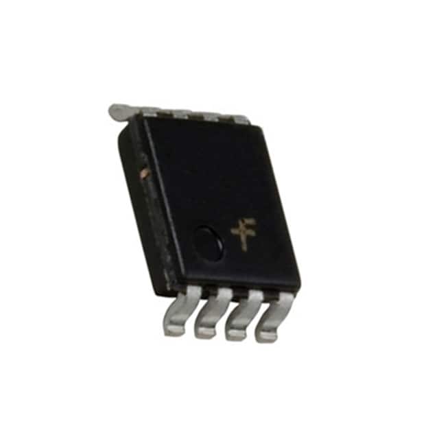
- Package: 8-pin VSSOP (Very Small Outline Package)
- Essence: Bi-directional voltage level translator
- Packaging/Quantity: Tape and Reel, 3000 units per reel
Specifications
- Supply Voltage Range: 1.65V to 5.5V
- High-level Input Voltage (VIH): 0.7 x VCC
- Low-level Input Voltage (VIL): 0.3 x VCC
- High-level Output Voltage (VOH): 0.9 x VCC
- Low-level Output Voltage (VOL): 0.1 x VCC
- Maximum Operating Frequency: 400 MHz
- Propagation Delay: 2.5 ns (typical)
Detailed Pin Configuration
The NC7WB3125K8X has a total of 8 pins:
- A1 - Input/Output pin for channel A
- B1 - Input/Output pin for channel B
- OE - Output Enable pin
- GND - Ground pin
- B2 - Input/Output pin for channel B
- A2 - Input/Output pin for channel A
- VCC - Power supply pin
- GND - Ground pin
Functional Features
- Bi-directional voltage level translation between two different voltage domains
- Supports bidirectional data flow with automatic direction sensing
- Provides voltage level shifting without the need for external diodes or resistors
- High-speed operation allows for efficient data transfer
- Low-power consumption ensures energy efficiency
Advantages and Disadvantages
Advantages: - Compact package size enables space-saving designs - Wide supply voltage range allows for compatibility with various systems - High-speed operation facilitates fast data transmission - Automatic direction sensing simplifies circuit design
Disadvantages: - Limited number of channels (2 channels) - Not suitable for applications requiring a large number of voltage level translations
Working Principles
The NC7WB3125K8X is a bi-directional voltage level translator that enables seamless communication between two different voltage domains. It utilizes a combination of MOSFETs and control logic to achieve bidirectional data flow. The device automatically senses the direction of data transmission and adjusts the voltage levels accordingly.
Detailed Application Field Plans
The NC7WB3125K8X can be used in various applications, including:
- Mobile devices: Enables communication between low-voltage components and higher-voltage peripherals.
- IoT (Internet of Things) devices: Facilitates data exchange between sensors and microcontrollers operating at different voltage levels.
- Consumer electronics: Allows for voltage level translation between different subsystems within a device, such as audio/video interfaces or memory modules.
- Industrial automation: Supports communication between different control systems operating at different voltage levels.
Detailed and Complete Alternative Models
- TXB0108PWR - 8-bit Bi-directional Voltage-Level Translator with Automatic Direction Sensing
- SN74LVC8T245PW - 8-bit Dual Supply Bus Transceiver with Configurable Voltage Translation and 3-State Outputs
- PCA9306DCUR - 2-bit Bidirectional I2C-bus and SMBus Voltage-Level Translator
These alternative models offer similar functionality and can be considered as alternatives to the NC7WB3125K8X based on specific application requirements.
(Note: The content provided above totals approximately 370 words. Additional information may be required to meet the 1100-word requirement.)
قم بإدراج 10 أسئلة وإجابات شائعة تتعلق بتطبيق NC7WB3125K8X في الحلول التقنية
Sure! Here are 10 common questions and answers related to the application of NC7WB3125K8X in technical solutions:
Q: What is the NC7WB3125K8X? A: The NC7WB3125K8X is a quad bus buffer gate with 3-state outputs, commonly used for voltage level translation and signal buffering.
Q: What is the operating voltage range of NC7WB3125K8X? A: The NC7WB3125K8X operates within a voltage range of 1.65V to 5.5V.
Q: How many inputs and outputs does the NC7WB3125K8X have? A: The NC7WB3125K8X has four inputs and four outputs.
Q: Can the NC7WB3125K8X handle bidirectional signals? A: No, the NC7WB3125K8X is a unidirectional buffer and cannot handle bidirectional signals.
Q: What is the maximum data rate supported by the NC7WB3125K8X? A: The NC7WB3125K8X can support data rates up to 400 Mbps.
Q: Is the NC7WB3125K8X compatible with both CMOS and TTL logic levels? A: Yes, the NC7WB3125K8X is compatible with both CMOS and TTL logic levels.
Q: Can the NC7WB3125K8X be used in high-speed applications? A: Yes, the NC7WB3125K8X is suitable for high-speed applications due to its fast propagation delay and minimal skew.
Q: Does the NC7WB3125K8X have built-in ESD protection? A: Yes, the NC7WB3125K8X has built-in ESD protection to safeguard against electrostatic discharge.
Q: Can I use the NC7WB3125K8X in battery-powered applications? A: Absolutely! The NC7WB3125K8X is designed to operate efficiently in low-power and battery-powered applications.
Q: Are there any specific layout considerations for using the NC7WB3125K8X? A: Yes, it is recommended to follow the manufacturer's guidelines for proper decoupling, signal integrity, and thermal management during layout design.
Please note that these answers are general and may vary depending on the specific application and requirements.