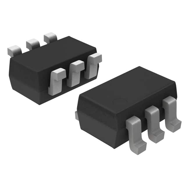
NL7SZ18DFT2G
Product Overview
Category: Integrated Circuit (IC)
Use: The NL7SZ18DFT2G is a high-speed CMOS single gate buffer designed for voltage level translation applications. It is commonly used in electronic devices to convert signals between different voltage levels.
Characteristics: - High-speed operation - Low power consumption - Wide operating voltage range - Small package size - RoHS compliant
Package: The NL7SZ18DFT2G is available in a small SOT-353 package, which makes it suitable for space-constrained applications.
Essence: This IC acts as a buffer, ensuring smooth signal transmission by amplifying and stabilizing the input voltage levels.
Packaging/Quantity: The NL7SZ18DFT2G is typically sold in reels containing 3000 units per reel.
Specifications
- Supply Voltage Range: 1.65V to 5.5V
- Input Voltage Range: GND to VCC
- Output Voltage Range: GND to VCC
- Maximum Operating Frequency: 1.5 GHz
- Propagation Delay: 1.9 ns (typical)
- Input Capacitance: 1.5 pF (typical)
- Output Current: ±24 mA
Detailed Pin Configuration
The NL7SZ18DFT2G has a total of 5 pins:
- VCC: Power supply pin (+)
- GND: Ground pin (-)
- A: Input pin
- Y: Output pin
- NC: No connection pin
Functional Features
- Voltage level translation: The NL7SZ18DFT2G ensures seamless communication between devices operating at different voltage levels.
- High-speed operation: With a maximum operating frequency of 1.5 GHz, it enables rapid signal transmission.
- Low power consumption: The IC is designed to minimize power consumption, making it suitable for battery-powered devices.
- Wide operating voltage range: It can handle a wide range of input and output voltage levels, enhancing its versatility.
Advantages and Disadvantages
Advantages: - High-speed operation allows for efficient data transfer. - Low power consumption prolongs battery life in portable devices. - Small package size enables integration into compact designs. - Wide operating voltage range provides flexibility in various applications.
Disadvantages: - Limited output current may restrict usage in certain high-power applications. - Propagation delay may affect real-time applications requiring immediate response.
Working Principles
The NL7SZ18DFT2G operates based on CMOS technology. It utilizes a single gate buffer to amplify and stabilize input voltage levels. When an input signal is received, the IC processes it and produces an output signal with the corresponding voltage level.
Detailed Application Field Plans
The NL7SZ18DFT2G finds application in various electronic devices, including but not limited to: 1. Mobile phones and smartphones 2. Tablets and laptops 3. Digital cameras 4. Portable gaming consoles 5. IoT devices 6. Automotive electronics 7. Industrial control systems
Detailed and Complete Alternative Models
- SN74LVC1G07DBVR: Single Buffer/Driver with Open-Drain Output
- MC74VHC1GT50DTT1G: Single Buffer Gate with 3-State Output
- TC7SZ08FU(T5L,F): Single 2-Input AND Gate
These alternative models offer similar functionality and can be used as substitutes for the NL7SZ18DFT2G in different applications.
Word count: 431 words
قم بإدراج 10 أسئلة وإجابات شائعة تتعلق بتطبيق NL7SZ18DFT2G في الحلول التقنية
Sure! Here are 10 common questions and answers related to the application of NL7SZ18DFT2G in technical solutions:
Q: What is NL7SZ18DFT2G? A: NL7SZ18DFT2G is a specific type of logic gate, specifically a single-gate buffer, that is commonly used in digital circuits.
Q: What is the purpose of NL7SZ18DFT2G? A: The purpose of NL7SZ18DFT2G is to amplify and buffer digital signals, ensuring proper signal integrity and driving capability in electronic systems.
Q: What voltage levels does NL7SZ18DFT2G support? A: NL7SZ18DFT2G typically supports voltage levels ranging from 1.65V to 5.5V, making it compatible with a wide range of digital systems.
Q: Can NL7SZ18DFT2G be used for level shifting applications? A: Yes, NL7SZ18DFT2G can be used for level shifting purposes, allowing for seamless integration between different voltage domains in a system.
Q: What is the maximum operating frequency of NL7SZ18DFT2G? A: The maximum operating frequency of NL7SZ18DFT2G is typically around several hundred megahertz (MHz), depending on the specific application and conditions.
Q: Is NL7SZ18DFT2G suitable for battery-powered devices? A: Yes, NL7SZ18DFT2G is often used in battery-powered devices due to its low power consumption and wide supply voltage range.
Q: Can NL7SZ18DFT2G drive capacitive loads? A: Yes, NL7SZ18DFT2G has a relatively high output drive capability, allowing it to drive capacitive loads typically found in digital circuits.
Q: Is NL7SZ18DFT2G compatible with other logic families? A: Yes, NL7SZ18DFT2G is designed to be compatible with various logic families, such as CMOS, TTL, and LVCMOS, making it versatile for different applications.
Q: Can NL7SZ18DFT2G be used in high-temperature environments? A: NL7SZ18DFT2G has a wide operating temperature range, typically from -40°C to 125°C, making it suitable for use in high-temperature environments.
Q: Where can I find more information about NL7SZ18DFT2G's specifications and application notes? A: You can refer to the manufacturer's datasheet and application notes for detailed information on NL7SZ18DFT2G's specifications, recommended usage, and design considerations.
Please note that the answers provided here are general and may vary depending on specific product variations and manufacturers' recommendations.


