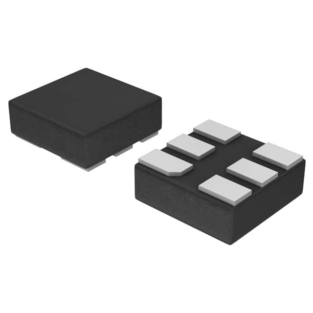
NLX2G07CMX1TCG
Product Overview
Category: Integrated Circuit (IC)
Use: The NLX2G07CMX1TCG is a dual buffer gate IC that is commonly used in digital logic circuits. It provides buffering and signal amplification capabilities, making it suitable for various applications in electronic devices.
Characteristics: - Low power consumption - High-speed operation - Wide operating voltage range - Small package size - RoHS compliant
Package: The NLX2G07CMX1TCG is available in a small outline package (SOT-353), which is compact and easy to handle. This package ensures efficient heat dissipation and protects the IC from external factors such as moisture and dust.
Essence: The essence of the NLX2G07CMX1TCG lies in its ability to amplify and buffer digital signals effectively, ensuring reliable and accurate data transmission within electronic circuits.
Packaging/Quantity: The NLX2G07CMX1TCG is typically sold in reels or tubes, with each reel or tube containing a specific quantity of ICs. The exact packaging and quantity may vary depending on the manufacturer and supplier.
Specifications
- Supply Voltage Range: 1.65V to 5.5V
- Input Voltage Range: 0V to VCC
- Output Voltage Range: 0V to VCC
- Operating Temperature Range: -40°C to +85°C
- Maximum Propagation Delay: 3.5 ns
- Maximum Quiescent Current: 1 µA
Detailed Pin Configuration
The NLX2G07CMX1TCG has a total of 6 pins, which are labeled as follows:
- A Input 1
- Y Output 1
- GND Ground
- B Input 2
- Y Output 2
- VCC Supply Voltage
Functional Features
- Dual buffer gate functionality
- High-speed operation for efficient signal transmission
- Low power consumption for energy-efficient designs
- Wide operating voltage range allows compatibility with various systems
- Schmitt-trigger input for improved noise immunity
- Open-drain outputs for flexible interfacing with other devices
Advantages and Disadvantages
Advantages: - Low power consumption makes it suitable for battery-powered devices - High-speed operation enables fast data processing - Wide operating voltage range ensures compatibility with different systems - Small package size saves board space in compact designs - RoHS compliant, environmentally friendly
Disadvantages: - Limited output current capacity - Not suitable for high-power applications
Working Principles
The NLX2G07CMX1TCG operates based on the principles of digital logic gates. It takes two input signals (A and B) and provides two buffered output signals (Y). The buffer gate amplifies and shapes the input signals to ensure proper signal levels and drive capability for subsequent stages in the circuit.
Detailed Application Field Plans
The NLX2G07CMX1TCG finds applications in various electronic devices and systems, including but not limited to: - Digital cameras - Mobile phones - Portable media players - Gaming consoles - Computer peripherals - Industrial control systems - Automotive electronics
Detailed and Complete Alternative Models
- SN74LVC2G07DBVR - Dual Buffer Gate IC by Texas Instruments
- MC74VHC1G07DTT1G - Single Buffer Gate IC by ON Semiconductor
- CD74HCT07M96 - Hex Buffer Gate IC by Texas Instruments
- 74HC07D - Hex Buffer Gate IC by NXP Semiconductors
- TC7SZ07FU - Dual Buffer Gate IC by Toshiba Semiconductor
These alternative models offer similar functionality and can be used as substitutes for the NLX2G07CMX1TCG in various applications.
Note: The above information is subject to change. Always refer to the manufacturer's datasheet for the most accurate and up-to-date specifications.
قم بإدراج 10 أسئلة وإجابات شائعة تتعلق بتطبيق NLX2G07CMX1TCG في الحلول التقنية
Sure! Here are 10 common questions and answers related to the application of NLX2G07CMX1TCG in technical solutions:
Q1: What is NLX2G07CMX1TCG? A1: NLX2G07CMX1TCG is a specific integrated circuit (IC) that belongs to the family of logic gates. It is a dual buffer with open-drain outputs.
Q2: What is the purpose of NLX2G07CMX1TCG? A2: The purpose of NLX2G07CMX1TCG is to provide buffering and signal amplification capabilities in digital circuits.
Q3: What voltage levels does NLX2G07CMX1TCG support? A3: NLX2G07CMX1TCG supports a wide range of voltage levels, typically from 1.65V to 5.5V.
Q4: Can NLX2G07CMX1TCG be used in both low-power and high-power applications? A4: Yes, NLX2G07CMX1TCG is designed to work efficiently in both low-power and high-power applications.
Q5: How many inputs and outputs does NLX2G07CMX1TCG have? A5: NLX2G07CMX1TCG has two inputs and two outputs.
Q6: What is the maximum operating frequency of NLX2G07CMX1TCG? A6: The maximum operating frequency of NLX2G07CMX1TCG is typically around 100 MHz.
Q7: Can NLX2G07CMX1TCG be used in both CMOS and TTL logic systems? A7: Yes, NLX2G07CMX1TCG is compatible with both CMOS and TTL logic systems.
Q8: What is the power supply voltage range for NLX2G07CMX1TCG? A8: The power supply voltage range for NLX2G07CMX1TCG is typically from 1.65V to 5.5V.
Q9: Can NLX2G07CMX1TCG be used in automotive applications? A9: Yes, NLX2G07CMX1TCG is suitable for automotive applications as it can withstand harsh environmental conditions.
Q10: Is NLX2G07CMX1TCG readily available in the market? A10: Yes, NLX2G07CMX1TCG is a commonly available IC and can be easily sourced from various electronic component suppliers.
Please note that the specific details mentioned above may vary depending on the manufacturer's specifications and datasheets.


